RAK3401 WisBlock BLE Module Datasheet
Overview
Description
The RAK3401 WisBlock Core module is a RAK3400 stamp module with an expansion PCB and connectors compatible with WisBlock Base Boards. It allows an easy way to access to the pins of the RAK3400 module in order to simplify development and testing processes.
The module itself comprises a RAK3400 as its main component. The RAK3400 is a based on the nRF52840 MCU, it features ultra-low power consumption of 2.0 uA during sleep mode, and the BLE interface with output power up to 4 dBm.
The RF communication characteristic of the module makes it suitable for a variety of applications in the IoT field such as home automation, sensor networks, building automation, personal area networks applications (health/fitness sensors, and monitors, etc.).
Features
- I/O ports: UART/I2C/GPIO/USB
- SPI pins and optional NFC interface are accessible using WisBlock IO module
- Temperature range: -40 °C to +85 °C
- Supply voltage: 2.0 ~ 3.6 V
- Low-Power Wireless Systems with 7.8 KHz to 500 KHz Bandwidth
- Ultra-Low Power Consumption 2.0 uA in sleep mode
- BLE5.0 (Tx power -20 to +4 dBm in 4dB steps)
- Serial Wire Debug (SWD) interface
- Module size: 20 x 30 mm
- Chipset: Nordic nRF52840
Specifications
Overview
The overview covers the RAK3401 board overview and the mounting mechanics of the board into the baseboard.
Board Overview
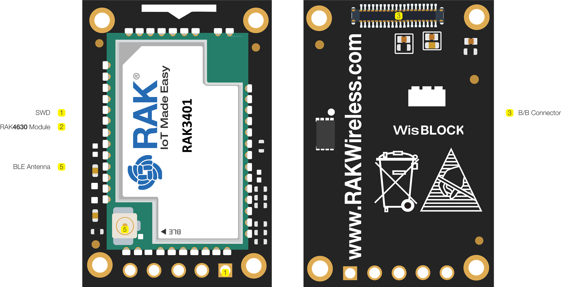 Figure 1: RAK3401 Overview
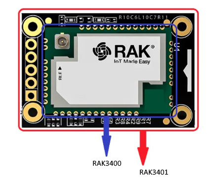 Figure 1: RAK3400 in RAK3401 WisBlock Core
Mounting Sketch
The RAK3401 module is designed to work with WisBlock Base Boards. Figure 3 shows how a RAK3401 module should be mounted on top of the RAK19007.
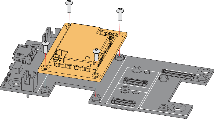 Figure 1: RAK3401 Mounting Sketch
Hardware
The hardware specification is categorized into four parts. It discusses the pinouts of the module and its corresponding functions and diagrams. It also covers the interfaces, RF, electrical, and mechanical parameters that include the tabular data of the functionalities and standard values of the RAK3401 Module.
Chipset
| Vendor | Part number |
|---|---|
| Nordic | nRF52840 |
Electrical Characteristics
Power Consumption
| Item | Power Consumption | Condition |
|---|---|---|
| Tx mode BT@4 dBm | 9 mA | BT Tx mode & Lora sleep |
| Rx mode BT@2 Mbps | 11.5 mA | BT Rx mode & Lora sleep |
| Sleep mode | 2.0 uA | LoRa&BT sleep |
Absolute Maximum Ratings
| Symbol | Description | Min. | Nom. | Max. | Unit |
|---|---|---|---|---|---|
| VDD_NRF | MCU power supply | -0.3 | 3.9 | V | |
| VBUS | USB supply voltage | -0.3 | 5.8 | V | |
| VBAT_NRF | MCU high voltage power supply | -0.3 | 5.8 | V |
Recommended Operating Conditions
| Symbol | Description | Min. | Nom. | Max. | Unit |
|---|---|---|---|---|---|
| VDD_NRF | NRF52840 power supply | 2.0 | 3.3 | 3.6 | V |
| VBUS | VBUS USB supply voltage | 4.35 | 5.0 | 5.5 | V |
| VBAT_NRF | NRF52840 high voltage power supply | 2.5 | 5.5 | V |
Schematic Diagram
 Figure 1: RAK3401 Schematic Diagram
-
WisConnector: The breakout module allows the RAK3400 stamp module pinout to be transferred by the board-to-board WisConnector.
-
WisConnector Pin Order: The pin order of the WisConnector is located in the bottom layer of the module.
-
Core Module: The breakout module itself has a RAK3400 at its core, and it shows the core module pin and connection information. By default, the NFC function is disabled for conserve the low power characteristic.
-
SWD Interface: The breakout module exposes a SWD debug interface. Additionally, the RST pin is used for resetting the core module RAK3400.
-
Power Up Automatic Reset: The breakout module has a power-up automatic reset circuit, and the schematic shows the automatic reset mechanism. This module also can be reset though WisBlock Base Board reset pin.
Mechanical Characteristics
Board Dimensions
 Figure 1: Mechanical Dimensions
WisConnector PCB Layout
 Figure 1: WisConnector PCB footprint and recommendations