RAK3172-SiP WisDuo LPWAN SiP Application Note
Overview
The RAK3172-SiP is a specialized WisDuo LPWAN module due to its SiP package. This document lists various hardware considerations and details to optimize module operation. It provides general information and guidelines for fine-tuning the module based on your application.
This document discusses the following:
Schematic Notes
RF Harmonic Compression
Place the harmonic suppression circuit close to the module's RF output. This might be necessary depending on your EMI test results. Default values are L102 = 8.2 nH Murata LQW15AN, C125 = 3.3 pF, and C126 = 3.3 pF.
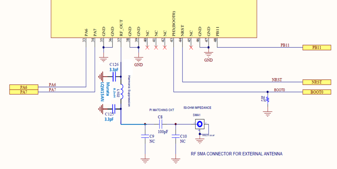 Figure 1: Harmonic Compression Circuit
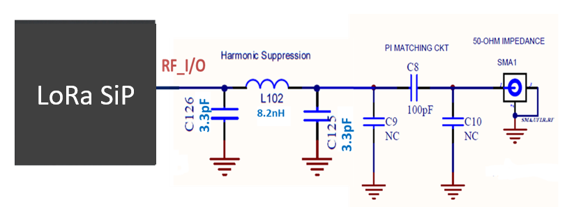 Figure 1: Harmonic Compression Circuit
RF Switch Control Table
PA0 and PA1 are internally connected and control the RF path.
| VC1(PA0) | VC2(PA1) | RF_TX-RF_ANT | RF_RX-RF_ANT |
|---|---|---|---|
| High | Low | Off | On |
| Low | High | On | Off |
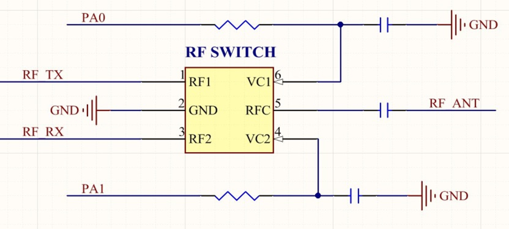 Figure 1: RF Switch
Power Considerations
An independent LDO Buck or Boost converter for Vin regulated to VDD (3.3 V) is recommended for RAK3172-SiP. Place the LDO Buck or Boost Converter as close as possible to the RAK3172-SiP power-related pins.
 Figure 1: Power pins
 Figure 1: Bypass Capacitors
Battery Protection
This is a safety feature you can add to the module. This will not affect the core functionality of the SiP module.
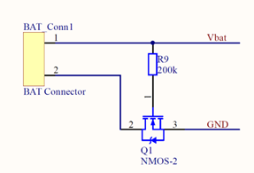 Figure 1: Battery Protection Circuit
Inductor Selection
The L1 (15 μH) consideration and recommendation:
- DCR (max) = 2 ohms
- Idc (min) = 100 mA
- Freq (min) = 20 MHz
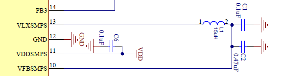 Figure 1: Inductor Selection
| Reference | Manufacturer | Value (uH) | Idc max (mA) | Freq (Mhz) | DCR (ohm) | Package (mm) |
|---|---|---|---|---|---|---|
| LPS3010-153 | Coilcraft | 15 | 370 | 43 | 0.95 | 2.95 x 2.95 x 0.9 |
| MLZ2012N150L | TDK | 15 | 90 | 40 | 0.47 | 2 x 1.25 x 1.25 |
| MLZ2012M150W | TDK | 15 | 120 | 40 | 0.95 | 2 x 1.25 x 1.25 |
| VLS2010ET-150M | TDK | 15 | 440 | 40 | 1.476 | 2 x 2 x 1 |
| VLS2012ET-150M | TDK | 15 | 440 | 40 | 1.062 | 2 x 2 x 1.2 |
ST-LINK SWD Port
Connect these three pins, SWDIO, SWCLK, and NRST, with the ST-LINK debugger.
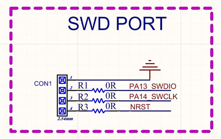 Figure 1: ST-Link Connection
NRST
The system reset is active low. Ensure to place R24/C16 as close as possible to the RAK3172-SIP module.
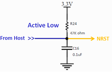 Figure 1: NRST pin
Power Supply Management
The RAK3172-SiP has two embedded regulators: one LDO and one DC/DC (SMPS). The SMPS can be optionally software-switched on to improve power efficiency. Because the LDO and SMPS operate in parallel, switching on the SMPS is transparent to the user and improves power efficiency. This section discusses internal and external details of the RAK3172-SiP's power supply.
Power Supply Voltages
The devices require a VDD operating voltage supply between 1.8 V and 3.6 V. Several independent supplies (VDDSMPS, VFBSMPS, VDDA, VDDRF) may be provided for specific peripherals.
- VDD = 1.8 V to 3.6 V
VDD is the external power supply for the I/Os, the system's analog blocks such as reset, power management, internal clocks, and low-power regulators. It is provided externally through VDD pins.
- VDDSMPS = 1.8 V to 3.6 V
VDDSMPS is the external power supply for the SMPS step-down converter. It is provided externally through the VDDSMPS supply pin and must be connected to the same supply as VDD.
- VFBSMPS = 1.45 V to 1.62 V (1.55 V typical)
VFBSMPS is the external power supply for the main system regulator. It is provided externally via the VFBSMPS pin and supplied through an SMPS step-down converter.
- VDDA = 0 V to 3.6 V
VDDA is the external analog power supply for A/D converters, D/A converters, voltage reference buffers, and comparators. The VDDA voltage level is independent of the VDD voltage (refer to the power-up and power-down sequence section) and should preferably be connected to VDD when these peripherals are not in use.
DAC minimum voltage is 1.71 V without buffer and 1.8 V with buffer. COMP and ADC minimum voltages are 1.62 V. VREFBUF minimum voltage is 2.4 V.
- VDDRF = 1.8 Vto 3.6 V
VDDRF is an external power supply for the radio. It is provided externally via the VDDRF pin and must be connected to the same supply as VDD.
- VBAT = 1.55 Vto 3.6 V
VBAT is the power supply for the RTC, TAMP, an external clock 32 kHz oscillator, and backup registers (through a power switch) when VDD is not present.
- VREF-, VREF+
VREF+ is the input reference voltage for ADC and DAC. It is also the output of the internal voltage reference buffer when enabled.
- When VDDA < 2 V, VREF+ must be equal to VDDA.
- When VDDA ≥ 2 V, VREF+ must be between 2 V and VDDA.
VREF+ can be grounded when ADC/DAC is not active. The internal voltage reference buffer supports the following output voltages, configured with VRS bit in the VREFBUF_CSR register:
- VREF+ around 2.048 V: this requires VDDA ≥ 2.4 V.
- VREF+ around 2.5 V: this requires VDDA ≥ 2.8 V.
Power Up and Down Sequence
During power up and power down, the following power sequence is required:
-
When VDD < 1 Vother, power supplies (VDDA) must remain below VDD + 300 mV. During power down, VDD can temporarily become lower than other supplies only if the energy provided to the device remains below 1 mJ. This allows external decoupling capacitors to be discharged with different time constants during this transient phase.
-
When VDD > 1 V, all other power supplies (VDDA) become independent. An embedded linear voltage regulator is used to supply the internal digital power VCORE. VCORE powers the digital peripherals, SRAM1 and SRAM2. The flash memory is powered by VCORE and VDD. VCORE is split into two parts: a VDDO part and an interruptible part, VDDI.
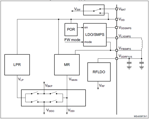 Figure 1: RAK3172-SiP Power Section
VDDPA
To transmit high output power up to + 22 dBm, VDDPA must be supplied directly from VDD on the VDDSMPS pin, as shown in Figure 11.
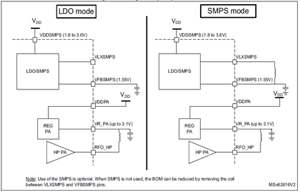 Figure 1: VDDPA Supply
The output power range is programmable in 32 steps of 1 dB. The power amplifier ramping timing is also programmable, allowing adaptation to meet radio regulation requirements. The table below gives the maximum transmitter output power versus the VDDPA supply level.
| VDDPA Supply (V) | Transmit Output Power (dBm) |
|---|---|
| 3.3 | +22 |
| 2.7 | +20 |
| 2.4 | +19 |
| 1.8 | +16 |
Power Supply Configurations
There are two different supply configurations, as shown in Figure 12.
- By the MCU using the SMPSEN setting in PWR control register 5 (PWR_CR5), which depends on the MCU system operating mode (Run, Stop, Standby, or Shutdown).
- By the sub-GHz radio using SetRegulatorMode() command and the sub-GHz radio operating mode (Sleep, Calibrate, Standby, Standby with HSE32 or Active).
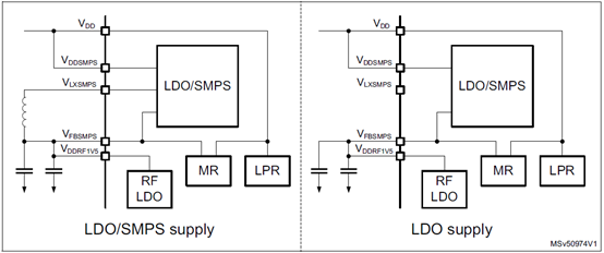 Figure 1: LDO and SMPS configurations
Power Supply Related Details
- After any POR and NRST reset, the LDO mode is selected. SMPS selection has priority over LDO selection.
- While the sub-GHz radio is in Standby with HSE32 or in Active mode, the supply mode is not altered until the sub-GHz radio enters Standby or Sleep mode. The sub-GHz radio activity may add a delay in entering the MCU software-requested supply mode.
- The LDO or SMPS supply mode can be checked with the SMPSRDY flag in power status register 2 (PWR_SR2).
- When the radio is active, the supply mode is not changed until the activity is finished.
- During Stop 1, Stop 2, and Standby modes, when the sub-GHz radio is not active, the LDO or SMPS step-down converter is switched off. When exiting low-power modes (except Shutdown), the SMPS step-down converter is set by hardware to the mode selected by the SMPSEN bit in power control register 5 (PWR_CR5). SMPSEN is retained in Stop and Standby modes.
- Independently of the MCU software-selected supply operating mode, the sub-GHz radio allows supply mode selection while active (possible due to the sub-GHz radio's SetRegulatorMode() command).
- The maximum load current delivered by the SMPS is selectable via the sub-GHz radio SUBGHZ_SMPSC2R register.
- The inrush current of the LDO and SMPS step-down converter is controllable via the sub-GHz radio SUBGHZ_PCR register. This information is retained in all modes except sub-GHz radio deep sleep mode.
- The SMPS requires a clock to function. If this clock stops, the device may be destroyed. To prevent this, clock detection is used to switch off the SMPS and enable the LDO in case of clock failure. The SMPS clock detection is enabled by the sub-GHz radio SUBGHZ_SMPSC0R.CLKDE bit. By default, SMPS clock detection is disabled and must be enabled before enabling the SMPS.
Before enabling the SMPS, the SMPS clock detection must be enabled in the Sub-GHz radio SUBGHZ_SMPSC0R.CLKDE.
Power Supply Supervisor
The module integrates a power-on/power-down reset, coupled with brownout reset (BOR) circuitry.
- BOR (Brownout Reset)
BOR0 level cannot be disabled. Other BOR levels can be enabled via user option. When enabled, BOR is active in all power modes except shutdown. Five BOR thresholds are selectable through option bytes.
During power-on, BOR keeps the device under reset until the supply voltage VDD reaches the specified VBORx threshold:
• When VDD drops below the selected threshold, a device reset is generated.
• When VDD is above the VBORx upper limit, the device reset is released and the system can start.
- PVD (Programmable Voltage Detector)
The module features an embedded programmable voltage detector (PVD) that monitors the VDD power supply and compares it with the VPVD threshold. An interrupt is generated when VDD drops below the VPVD threshold or when VDD is higher than the VPVD threshold. The interrupt service routine can then generate a warning message or put the MCU into a safe state.
The PVD is enabled by software and can be configured to monitor the VDD supply level needed for sub-GHz radio operation. For this, the PVD must select its lowest threshold, and the PVD and wakeup must be enabled by the EWPVD bit in the PWR_CR3 register. Only a voltage drop below the PVD level generates a wakeup event.
- PVM (Peripheral Voltage Monitor)
The module features an embedded PVM (peripheral voltage monitor) that compares the independent supply voltage VDDA with a fixed threshold to ensure that the peripheral is within its functional supply range.
- Radio End-Of-Life Monitor
A radio end-of-life monitor provides information on the VDD supply when VDD is too low to operate the sub-GHz radio. When reaching the EOL level, the software must safely stop all activity.
Linear Voltage Regulator
Two embedded linear voltage regulators supply all digital circuitry, except for the standby circuitry and the backup domain. The main regulator (MR) output voltage (VCORE) can be programmed by software to two different power ranges (range 1 and range 2) to optimize consumption depending on the system's maximum operating frequency. The voltage regulators are always enabled after a reset. Depending on the application mode, the VCORE supply is provided by either the main regulator or the low-power regulator (LPR).
When MR is used, a dynamic voltage scaling is proposed to optimize power as follows:
-
Range 1: High-performance range
- The system clock frequency can be up to 48 MHz.
- The Flash memory access time for read access is minimized.
- Write and erase operations are possible.
-
Range 2: Low-power range
- The system clock frequency can be up to 16 MHz.
- The flash memory access time for read access is increased as compared to range 1.
- Write and erase operations are possible.
VBAT
- VBAT Operation
The VBAT pin powers the device's VBAT domain (RTC, LSE, and backup registers) from an external battery, an external supercapacitor, or VDD when neither an external battery nor an external supercapacitor is present. Three anti-tamper detection pins are available in VBAT mode. VBAT operation activates automatically when VDD is absent.
An internal VBAT battery charging circuit is embedded and activates when VDD is present.
When the microcontroller is supplied only from VBAT, external interrupts, and RTC alarms/events do not exit it from VBAT operation.
- VBAT Battery Voltage Monitoring
This embedded hardware feature allows the application to measure the VBAT battery voltage using the ADC's VIN[14] input channel. Because VBAT may be higher than VDDA, and thus outside the ADC's input range, the VBAT pin is internally connected to a resistor divider. As a consequence, the converted digital value is one-third the VBAT voltage.
Low-Power Modes
The module supports several low-power modes to achieve the best compromise between low power consumption, short startup time, available peripherals, and available wake-up sources. By default, the microcontroller is in Run mode, range 1, after a system or power-on reset. It is up to the user to select one of the low-power modes described below:
- Sleep Mode:
CPU clock off; all peripherals, including CPU core peripherals (such as NVIC, SysTick), can run and wake the CPU when an interrupt or event occurs.
- Low-Power Run Mode (LPRun):
When the system clock frequency is reduced below 2 MHz, the code is executed from the SRAM or the Flash memory. The regulator is in low-power mode to minimize the operating current.
- Low-Power Sleep Mode (LPSleep):
Entered from the LPRun mode.
- Stop 0 and Stop 1 Modes:
The contents of SRAM1, SRAM2, and all registers are retained. All clocks in the VCORE domain are stopped. The PLL, MSI, HSI16, and HSE32 are disabled. LSI and LSE may remain active. The RTC may remain active (Stop mode with RTC, Stop mode without RTC). The sub-GHz radio may remain active independently of the CPU. Some peripherals with wake-up capability may enable the HSI16 RC during Stop mode to detect their wake-up conditions.
- Stop 1 Mode:
Stop 1 offers the largest number of active peripherals and wake-up sources, a smaller wake-up time, but higher consumption compared with Stop 2. In Stop 0 mode, the main regulator remains on, resulting in the fastest wake-up time but much higher consumption. The active peripherals and wake-up sources are the same as in Stop 1 mode, which uses the low-power regulator. When exiting Stop 0 or Stop 1 mode, the system clock can be either MSI up to 48 MHz or HSI16, depending on the software configuration.
- Stop 2 Mode:
In Stop 2 mode, part of the VCORE domain is powered off. Only SRAM1, SRAM2, the CPU, and some peripherals retain their contents. All clocks in the VCORE domain are stopped. The PLL, MSI, HSI16, and HSE32 are disabled.
LSI and LSE may remain active. The RTC may remain active (Stop 2 mode with RTC, Stop 2 mode without RTC). The sub-GHz radio may also remain active independently of the CPU. Some peripherals with wake-up capability may enable the HSI16 RC during Stop 2 mode to detect their wake-up condition. The system clock, when exiting Stop 2 mode, may be either MSI (up to 48 MHz) or HSI16, depending on the software configuration.
- Standby Mode:
The VCORE domain is powered off. However, SRAM2 content can be preserved as follows:
• Standby mode with SRAM2 retention: Set the RRS bit in PWR control register 3 (PWR_CR3). SRAM2 is supplied by the low-power regulator. Standby mode without SRAM2 retention: Clear the RRS bit in PWR_CR3. The main and low-power regulators are powered off. All VCORE domain clocks (PLL, MSI, HSI16, and HSE32) stop. LSI and LSE may remain active.
• The RTC may remain active (Standby mode with or without RTC). The sub-GHz radio and PVD may also remain active if enabled independently. In Standby mode, the PVD uses its lowest level. Upon exiting Standby mode, the system clock is MSI at 4 MHz.
- Shutdown Mode:
The VCORE domain is powered off. All clocks in the VCORE domain are stopped. The PLL, MSI, HSI16, LSI, and HSE32 are disabled. The LSE can be kept running. The system clock when exiting shutdown mode is the MSI at 4 MHz. In this mode, supply voltage monitoring is disabled, and product behavior is not guaranteed in case of a power voltage drop.
Layout Guideline
-
Power Trace Management
- Power traces should be directly connected to the regulator outputs, and then add 4.7 µF bypass capacitors close to the module on each power trace.
- Never let power traces cross each other or high-speed signal traces.
-
Ground Management
- Ensure (1) GND polygon regions used for the module are as complete as possible and (2) well-established GND via holes are present, to maintain good heat dissipation and RF performance.
- The reference ground planes of RF traces need additional via holes; we recommend a distance between each of less than 1/8 λ.
-
RF Trace Management
- The CPWG model is recommended for RF trace calculation because of its superior EMC and RF capabilities. Also, discuss with the PCB manufacturer how to evaluate and maintain the RF trace at 50 Ω.
- The recommended layout for RF trace bends is to maintain the same width in the corner.
 Figure 1: RF Trace
- The values of a and b will affect each other, it is best to control it not to be too wide from the width and gap of the output pad of the module
 Figure 1: PCB RF Trace
 -
RF Matching Circuit
- In Pi-matching circuits, it is advised to place them close to the LoRa antenna. For 50 Ω matching antenna applications, connect a 100 pF capacitor to the RF trace.
 Figure 1: Pi-matching Circuit
- If you choose a metal coil antenna, the impedance will be lower ( < 50 Ω) and it is inductive. Its R+jL is easier to fall on the upper left of the Smith Chart, so series inductance and parallel capacitance are the chosen matching method, but sometimes for bandwidth consideration, multi-level matching is also used.
 Figure 1: Matching Circuit for Coil Antenna
 -
ESD Protection If used in a harsh ESD environment, the following example is a reference design for ESD protection. The recommended part is Semtech - Rclamp2451z (1-Line, 24 V).
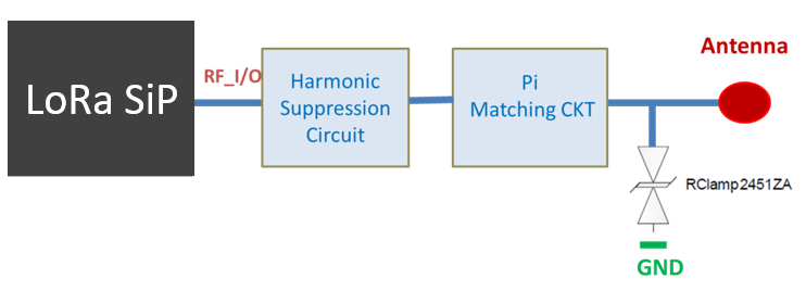 Figure 1: ESD Protection
- Shielding Cover
- Shielding Cover design is recommended for EMI suppression.
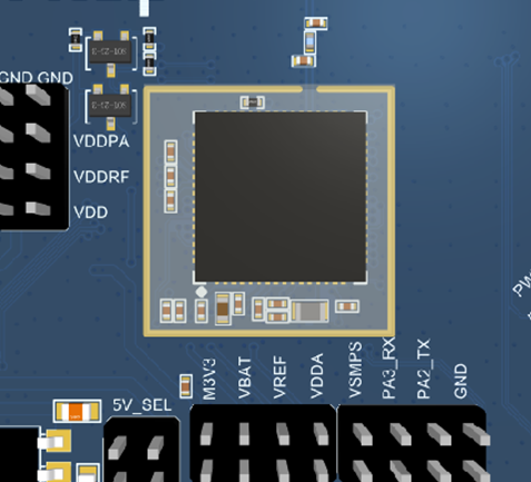 Figure 1: EMI Sheild