RAK4270 WisDuo LPWAN Module Datasheet
Overview
Description
The RAK4270 LoRa Module includes an STM32L071 MCU and an SX1262 LoRa chip, which supports eight (8) spreading factors (SF5 ~ SF12) and signal bandwidth that can be adjusted between 7.8 kHz to 500 kHz. It has Ultra-Low Power Consumption of 2.31 μA (down to 1.61 μA @ 2.0 V) in sleep mode, but during the Transmit Mode, it can reach the maximum output power of 22 dBm. As a receiver, it can achieve a sensitivity of -148 dBm.
The module complies with Class A and C of LoRaWAN 1.0.2 specifications, and it also supports LoRa Point-to-Point (P2P) communications. The module is suitable for various applications that require long-range data acquisition and low power consumption, such as smart meters, supply chain and logistics tracking, agricultural sensors, and smart cities.
You can configure the mode and operation of the RAK4270 module using RAK4270 AT Commands via a UART interface. Also, it offers low-power features that are very suitable for battery-powered applications.
Product Features
- LoRa module is suitable for applications in Smart City, Smart Agriculture, Smart Industry
- Compact form factor: 15 x 15.5 x 2.5 mm (LxWxH)
- 20 pin stamp pad for PCB SMT board-to-board soldering
- I/O ports: UART/I2C/GPIO/ADC
- AT commands control interface
- Temperature range: -30° C to +85° C
- Supply voltage: 2.0 to 3.6 V
- Supported bands: (EU433, CN470, IN865, EU868, AU915, US915, KR920, and AS923-1/2/3/4)
- LoRa bandwidth range of 7.8 kHz to 500 kHz, SF5 to SF12, BR=0.018~62.5 kb/s
- Ultra-Low Power Consumption of 2.31 μA (down to 1.61 μA @ 2.0 V) in sleep mode
- ARM Cortex-M0+ 32-bit RISC core
- 128 kbytes flash memory with ECC
- 20 kbytes RAM
- 6 kbytes of data EEPROM with ECC
Specifications
Overview
The overview shows the module top view and its block diagram where the core and external interfaces of the module are shown.
Board Overview
Figure 1 shows the top view of the RAK4270 LoRa module. The dimensions of the module are 15 x 15.5 x 2.5 mm
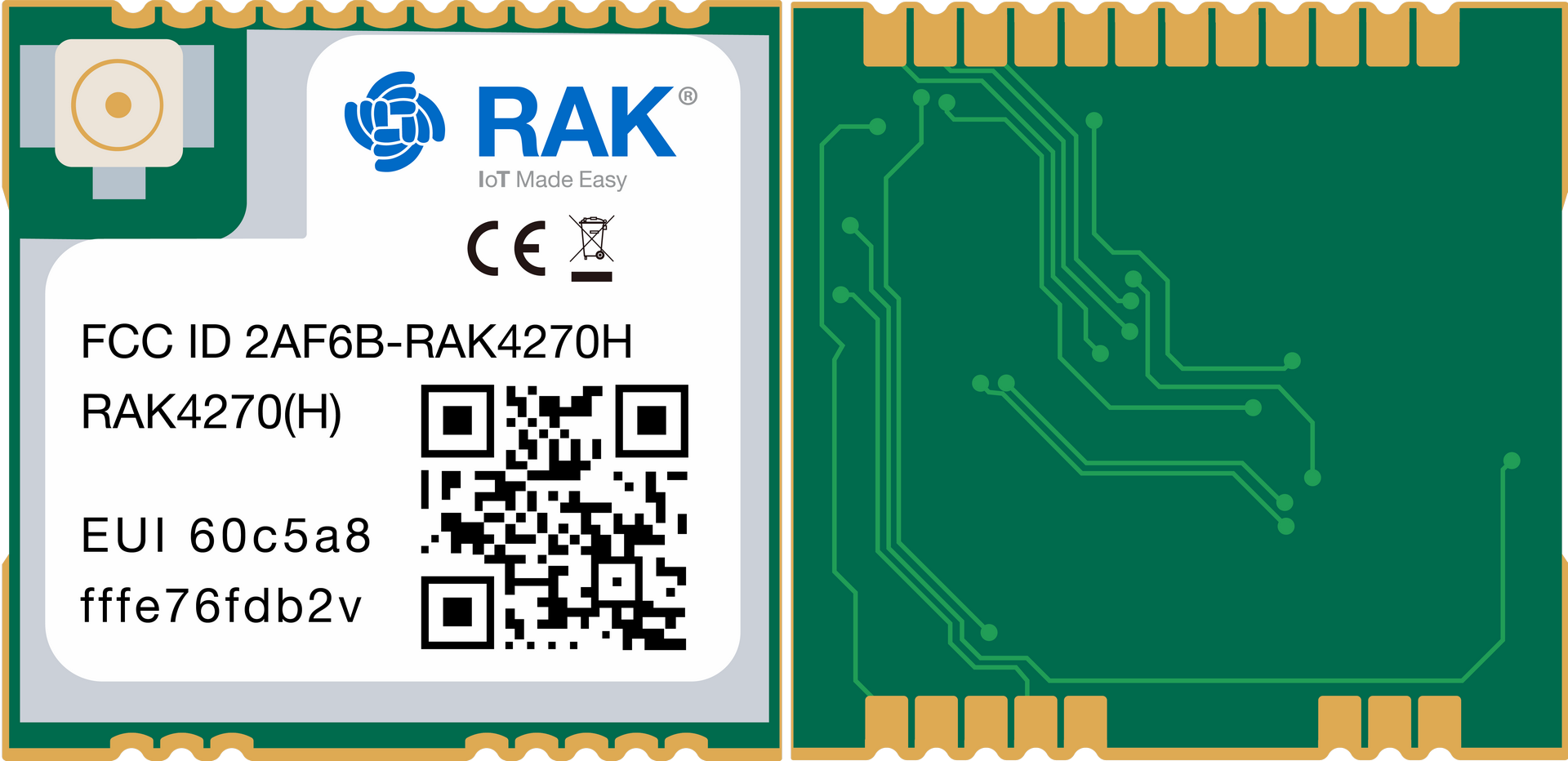 Figure 1: RAK4270 Module
Block Diagram
The block diagram representing the RAK4270 LoRa module is shown in Figure 2. External interfaces are outlined in the diagram.
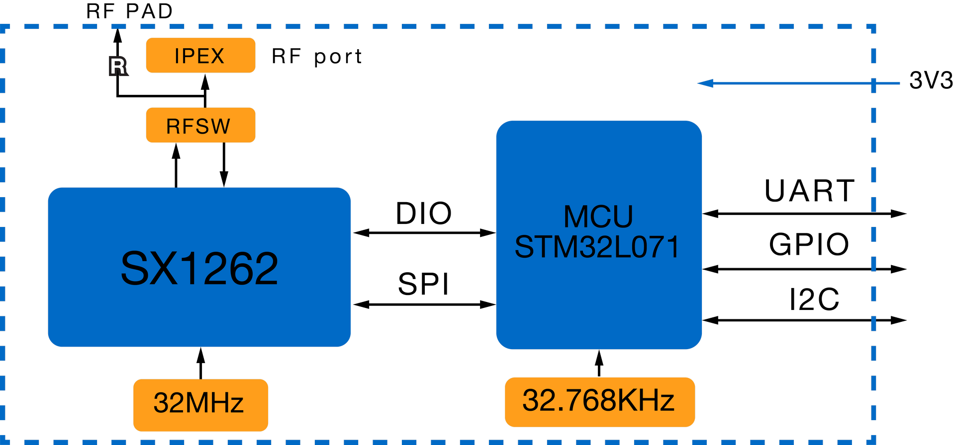 Figure 1: RAK4270 Module
Hardware
The hardware specification discusses the interfaces, pinouts and its corresponding functions and diagrams. It also covers the parameters of the RAK4270 Module in terms of RF, electrical, mechanical, and environmental characteristics.
Interfaces
| Module | Interfaces |
|---|---|
| RAK4270 | UART1, UART2, I2C, GPIO |
Pin Definition
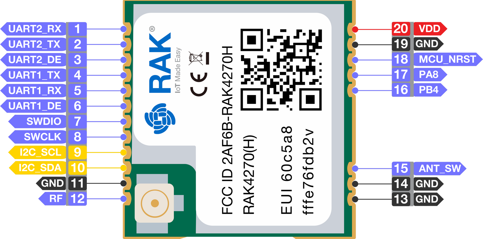 Figure 1: RAK4270 Pinout
When using RF pin for antenna and not the IPEX connector variant, there are design considerations to make sure optimum RF performance.
- RF trace must be away from interference (switching node of DC-DC supply, high current/voltage pulses from controllers of inductive load like motor, signal generators, etc.)
- RF trace must have 50 Ohms impedance. It is advisable to use an impedance simulation software tool to achieve this requirement.
- If using an external antenna connector, make it close to the
RFpin. - Ground plane optimization is critical on certain antenna types like monopole.
- GND trace used for RF path return must be directly connected to the GND plane and not be treated as thermal relief.
- It is recommended for the RF trace to be routed in a curve and not in a sharp 90 degrees.
In addition, with a commitment to making IoT easy, RAK offers a dedicated service for Antenna RF Design which includes PCB design, tuning, matching, and RF testing.
| Pin | Name | Type | Description | Alternate Functions |
|---|---|---|---|---|
| 1 | PA3/UART2_RX | I | UART2 Interface (AT Commands) | TIM21_CH2, TIM2_CH4, USART2_RX, LPUART1_RX |
| 2 | PA2/UART2_TX | O | UART2 Interface (AT Commands) | TIM21_CH1, TIM2_CH3, USART2_TX, LPUART1_TX, COMP2_OUT |
| 3 | PA1 | I/O | GPIO | EVENTOUT, TIM2_CH2, USART2_RTS/ USART2_DE, TIM21_ETR, USART4_RX |
| 4 | PA9/UART1_TX | I/O | UART1 Interface (AT Commands and FW Update) | MCO, USART1_TX, I2C1_SCL, I2C3_SMBA |
| 5 | PA10/UART1_RX | I/O | UART1 Interface (AT Commands and FW Update) | USART1_RX, I2C1_SDA |
| 6 | PA12/UART1_DE | I/O | GPIO | SPI1_MOSI,EVENTOUT, USART1_RTS/ USART1_DE, COMP2_OUT |
| 7 | PA13/SWDIO | I/O | SWD debug pin (SWDIO) | SWDIO, LPUART1_RX |
| 8 | PA14/SWCLK | I/O | SWD debug pin (SWCLK) | SWCLK, USART2_TX, LPUART1_TX |
| 9 | PB6/I2C_SCL | I/O | I2C interface | USART1_TX, I2C1_SCL, LPTIM1_ETR |
| 10 | PB7/I2C_SDA | I/O | I2C interface | USART1_RX, I2C1_SDA, LPTIM1_IN2, USART4_CTS |
| 11 | GND | Ground | ||
| 12 | RF | I/O | RF port (only available on RAK4270 No-IPEX connector variant) | |
| 13 | GND | Ground | ||
| 14 | GND | Ground | ||
| 15 | PA11/ANT_SW | I/O | ANT_SW | leave it unconnected on mainboard |
| 16 | PB4 | I/O | GPIO | SPI1_MISO, TIM3_CH1, TIM22_CH1, USART1_CTS, USART5_RX, I2C3_SDA |
| 17 | PA8 | I/O | GPIO | MCO, EVENTOUT, USART1_CK, I2C3_SCL |
| 18 | MCU_NRST | I/O | MCU reset (STM32L071KBU6 NRST) | |
| 19 | GND | Ground | Ground | |
| 20 | VDD | DC3V3 | Supply voltage 2.0~3.3 V |
LoRa Transceiver IC Connection to RAK4270 Internal STM32
| LoRa IC Pin | STM32 GPIO |
|---|---|
| DIO1 | PB1 |
| DIO2 | PB5 |
| SPI1_SCK | PA5 |
| SPI1_MISO | PA6 |
| SPI1_MOSI | PA7 |
| SPI1_NSS | PA4 |
| BUSY | PB0 |
| NRESET | PA0 |
| ANT_SW | PA11 |
RF Switch Control Logic table
| ANT_SW | DIO2 | Condition |
|---|---|---|
| 1 | 0 | RX mode |
| 0 | 1 | TX mode |
- Set Dio2AsRfSwitchControl = false
- Set Dio3AsTxcoControl = enable
SWD Programming Tool
To upgrade the firmware, the SWD (Serial Wire Debug) interface must be used. A 5-pin JLINK cable has to be connected to the SWD port. These pins are 3v3, GND, SWDIO, SWCLK, and MCU_NRST.
UARTS Ports
There are two UART ports on the RAK4270 module. UART2 (pin1 and pin2) can be used as the AT command port, while UART1 (pin4 and pin5) can be used both as AT command port and firmware upgrade port. It is recommended to connect the UART2 port to an external MCU and reserve UART1 for debugging and or future firmware upgrade purposes.
I2C Port
The RAK4270 exposes an I2C port, in which the SDA line is assigned to pin9, and the SCL line is assigned to pin10. This I2C port allows you to control additional slave sensors with the RAK4270 using the I2C protocol. The RAK4270 will be the master. If the I2C port is used, then external pull-up resistors must be added to the SDA and SCL lines. The recommended value of the resistors is 10 kΩ. You can develop your own firmware or use the RUI (RAKwireless Unified Interface) Online compiler to use this port.
RF Port
The RAK4270 module exposes two types of RF antenna: IPEX and PAD. The most straightforward way is to use the IPEX antenna port. In such a case, you just connect the antenna to the IPEX connector on the module directly. On the other hand, for specific needs, you can design a PCB trace antenna, Chip antenna, SMA antenna, or spring type antenna. In the latter case, you should use the PAD-type antenna port exposed by this module. The external antenna should be matched to the 50 Ω RF transmission line.
VDD Power In
It is recommended to add four decoupling capacitors near the RAK4270 power supply pins. The recommended values of the capacitors are two 10 uF and two 100 nF connected in parallel.
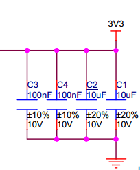 Figure 1: RAK4270 VDD port
RF Characteristics
Operating Frequencies
| Module | Region | Frequency |
|---|---|---|
| RAK4270(L) | Europe | EU433 |
| China | CN470 | |
| RAK4270(H) | Europe | EU868 |
| North America | US915 | |
| Australia | AU915 | |
| Korea | KR920 | |
| Asia | AS923 | |
| India | IN865 |
Electrical Characteristics
Schematic Diagram
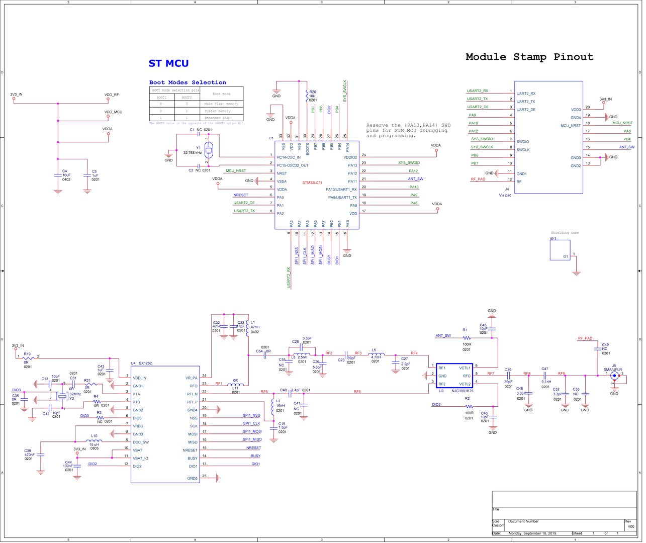 Figure 1: RAK4270 Schematic Diagram
Operating Voltage
| Feature | Minimum | Typical | Maximum | Unit |
|---|---|---|---|---|
| VCC | 2.0 | 3.3 | 3.6 | Volts (V) |
Operating Current
| Feature | Condition | Minimum | Typical | Maximum | Unit |
|---|---|---|---|---|---|
| Operating Current | TX Mode | 35.4 (@ 1 dBm SF7 868Mhz) | mA | ||
| RX Mode | 15.8 | mA |
Sleep Current
| Feature | Condition | Minimum (2.0V) | Typical (3.3V) | Maximum | Unit |
|---|---|---|---|---|---|
| Current Consumption | EU868 | 1.74 | 2.19 | μA | |
| US915 | 1.61 | 2.31 | μA |
Mechanical Characteristics
Dimensions
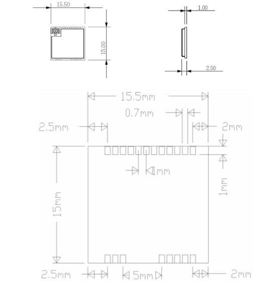 Figure 1: RAK4270 Mechanical Dimensions
Recommended Footprint
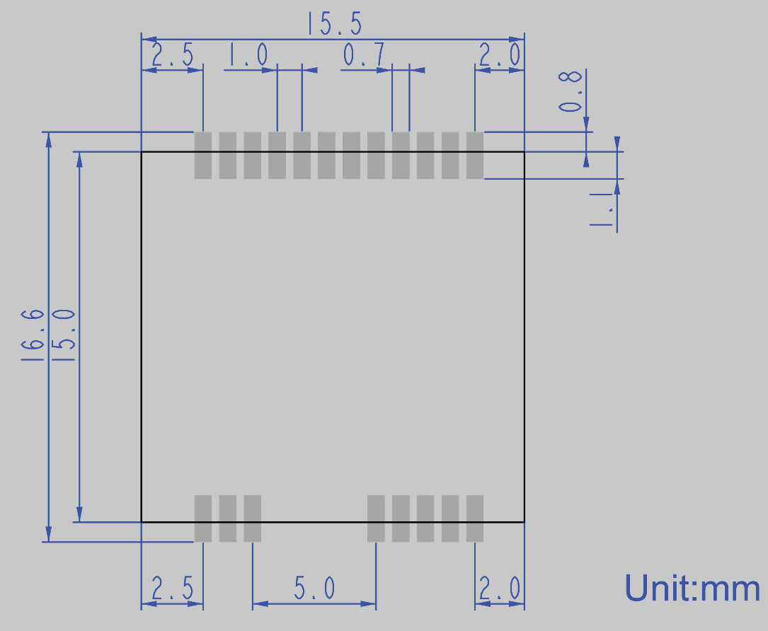 Figure 1: RAK4270 Recommended PCB footprint
Environmental Characteristics
Operating Temperature
| Feature | Minimum | Typical | Maximum | Unit |
|---|---|---|---|---|
| Operating Temperature | -30 | 25 | 85 | °C |
Storage Temperature
| Feature | Minimum | Typical | Maximum | Unit |
|---|---|---|---|---|
| Storage Temperature | -40 | 85 | °C |
Recommended Reflow Profile
- MSL Rating : Class 3
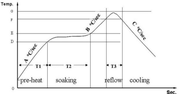 Figure 1: RAK4270 Recommended Reflow Profile
Standard conditions for reflow soldering:
- Pre-heating Ramp (A) (Initial temperature: 150 ℃): 1~2.5 ℃/sec
- Soaking Time (T2) (150
180 ℃): **60100 sec** - Peak Temperature (G): 230~250 ℃
- Reflow Time (T3) (>220 ℃): 30~60 sec
- Ramp-up Rate (B): 0~2.5 ℃/sec
- Ramp-down Rate (C): 1~3 ℃/sec
Software
Download the latest firmware of the RAK4270 WisDuo LPWAN Module as provided in the table below.
The bin file contains the application code only, and you need the RAK DFU Tool to upload this file to the module.
The hex file contains both the bootloader and the application code. You need to use STM32CubeProgrammer to upload this.
Firmware
| Model | Version | Source |
|---|---|---|
| RAK4270 | v3.3.0.18 |
