RAK19001 WisBlock Dual IO Base Board Datasheet
Overview
Description
RAK19001 is a WisBlock Base board that connects WisBlock Core and WisBlock Modules. It provides the power supply and interconnection to the modules attached to it. It has one slot reserved for the WisBlock Core module, two IO slots, and six sensor slots A to F for WisBlock Modules. Also, there are two 2.54 mm pitch headers that expose all key input-output pins of the WisBlock Core that includes UART, I2C, SPI, and many IO Pins.
For convenience, there is a Type-C USB connector that is connected directly to WisBlock Core MCU’s USB port (if supported) or to a USB-UART converter depending on the WisBlock Core. The USB-C connection can be used for uploading firmware, serial communication, and charging A rechargeable battery. RAK19001 also includes a slide switch to select between rechargeable and non-rechargeable batteries.
WisBlock Modules are connected to the RAK19001 WisBlock Base board via high-speed board-to-board connectors. They provide secure and reliable interconnection to ensure the signal integrity of each data bus. A set of screws are used for fixing the modules, which makes it reliable even in an environment with lots of vibrations.
Additionally, it has two user-definable LEDs, one power supply/charging indicator LED, and one user-defined button.
If you can't find a module that fits your IoT requirements, use the standard connectors of WisBlock to develop your own specific function module. WisBlock supports open-source hardware architecture and you can find tutorials showing how to create your own Awesome WisBlock module.
Features
- Flexible building block design, which enables modular functionality and expansion
- High-speed interconnection connectors in the WisBlock Base board to ensure signal integrity
- Multiple headers and modules slots for WisBlock modules
- Two (2) IO slots
- Six (6) sensor (A to F) slots
- All key input-output pins of WisBlock Core are exposed via headers
- Access to various communication bus via headers: I2C, SPI, UART, and USB
- One user-defined push button switch
- Power supply
- Supports both 5 V USB, 3.7 V rechargeable battery, and 3.3 to 5.5 V non-rechargeable battery as power supply
- The power supply for the WisBlock modules boards can be controlled by the WisBlock Core modules to minimize power consumption
- Slide switch to select between a rechargeable or non-rechargeable battery
- Size
- 60 x 67 mm
Specifications
Board Overview
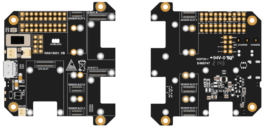 Figure 1: RAK19001 WisBlock Base top (left) and bottom (right) view
Block Diagram
The block diagram in Figure 2 shows the internal architecture and external interfaces of the RAK19001 board.
 Figure 1: RAK19001 WisBlock Base block diagram
Hardware
The hardware specification is categorized into six (6) parts. It discusses the interfacing, pinouts, and their corresponding functions and diagrams. It also covers the electrical, mechanical, and environmental parameters that include the tabular data of the functionalities and standard values of the RAK19001 WisBlock Dual IO Base Board.
Interfaces
RAK19001 WisBlock Base board provides the following interfaces, headers, a button, and WisConnectors:
- 1 WisBlock Core module
- 2 IO slots for WisBlock modules
- 6 Sensor slots A-F for WisBlock modules
- 1 Type-C USB port for programming and debugging
- 3.7 V rechargeable battery connector
- Non-rechargeable battery connector
- 5 V Solar panel connector
- 2 Headers for complete access to BOOT, I2C, SPI, UART, USB, and IO pins
- 2 User-defined LEDs
- 1 Power supply/charging indicator LED
- 1 User-defined button
- 1 Reset button
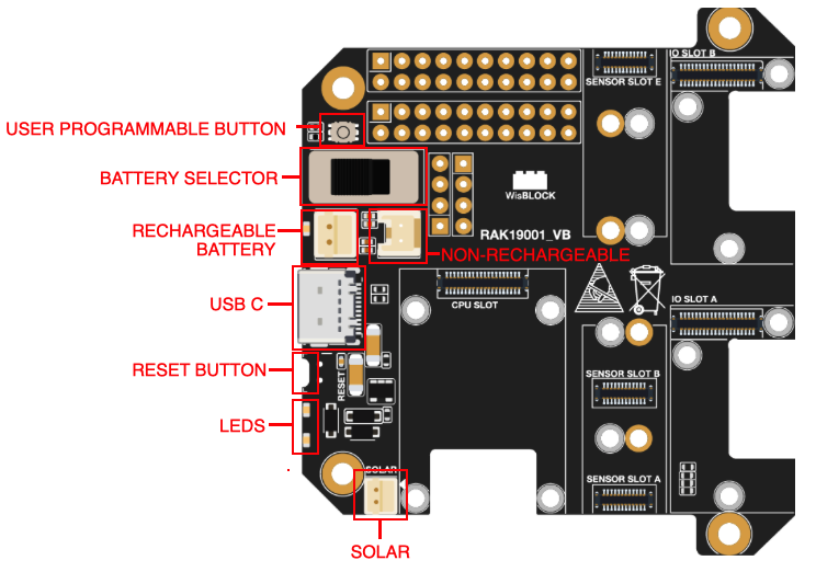 Figure 1: RAK19001 part labels
Type-C USB Port
The Type-C USB connector is compliant with the USB 2.0 specification. This USB interface directly communicates with the connected WisBlock Core module. It is also used as a charging input port for the battery. Here are some of the advantages of the Type-C USB connector:
- Smaller and reversible connector shape
- Port can be input or output
- Fast battery charging
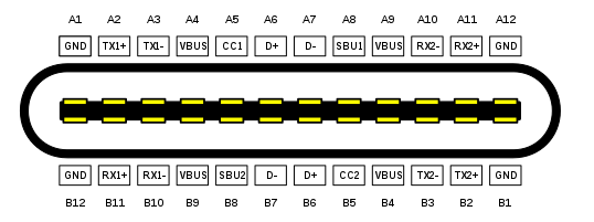 Figure 1: USB Type-C receptacle pinout
J10 and J15 Headers (Core IO Pins)
On the WisBlock Dual IO Base board, there are a total of 40 2.54 mm pitch headers for IO access and extension. These IO pins are distributed to J10 and J15 pin headers with the corresponding label at the back of the board. The arrangement of the pins is based on the 40-pin WisConnector of the WisBlock Core.
BOOT pin is used on startup configuration or sequence of the WisBlock Core connected to it. It is commonly used for uploading the bootloader and/or application firmware. The requirements of the state of the BOOT pin depend on the specific model of the WisBlock Core used.
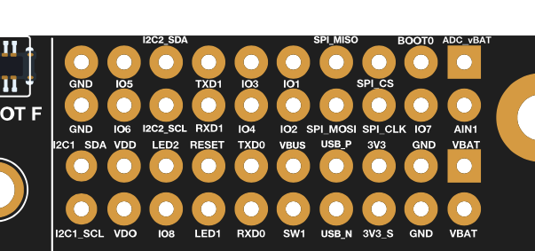 Figure 1: J10 and J15 pin header label in bottom side
J11 and J12 Headers (I2C and UART)
A dedicated header is available as well to have access to commonly used serial interfaces I2C and UART.
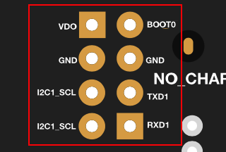 Figure 1: J11 and J12 (I2C and UART) pin header label in bottom side
Battery Connectors
Figure 7 and Figure 8 show the battery connectors V+(positive) and GND on both rechargeable and non-rechargeable batteries.
The matching connector for the rechargeable battery wires is a JST PHR-2 2 mm pitch female. A cable assembly for the rechargeable battery connector is also available for purchase in RAK store.
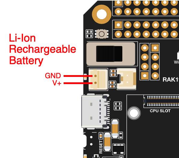 Figure 1: Rechargeable battery connector pin label V+ and GND
The onboard connector used on the non-rechargeable battery is FWF20009-S02S22W1B. The matching connector housing is FHG20005-S02M2W1B, and the connector tin-plate pin is FT20004-F2H.
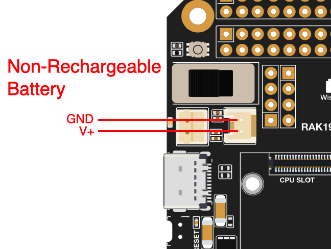 Figure 1: Non-Rechargeable battery connector pin label V+ and GND
Figure 9 shows how to select the battery type used for the project. The battery selector is based on the SS-12D10 slide SPDT switch. You can also use this slide switch as a power on/off switch to disconnect the battery from the board.
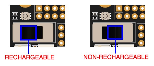 Figure 1: Battery selector switch
- The voltage of the rechargeable battery must not exceed 4.3 V.
- The voltage of the non-rechargeable battery must not exceed 5.5 V.
Solar Panel Connector
Figure 10 shows the solar panel connector V+(Vin) and GND. The matching connector for the solar panel wires is an JST ZHR-2 1.5 mm pitch female. A cable assembly for the solar panel connector is also available for purchase in RAK store.
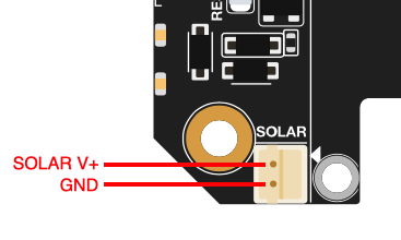 Figure 1: Solar panel connector V+ and GND
The output voltage of the solar panel must not exceed 5.5 V. Otherwise, it may cause permanent damage to the board.
LEDs
Three LEDs are used to indicate the operating status. Below are the functions of the LEDs:
- 🔴 Red LED - Connected to the charger chip to indicate the charger status. When the battery is charging, this red LED is on. When the battery is full, this LED is weak light or off.
- 🟢 Green LED - Connected to the MCU module, controlled by MCU defined by the user.
- 🔵 Blue LED - Connected to the MCU module, controlled by MCU defined by the user.
RESET Push Button
The Reset Push Button shown in Figure 3 of interfaces section is connected to the MCU module. When pushed, it resets the MCU.
User Programmable Push Button
The User Programmed Push Button shown in Figure 3 of interfaces section is connected to the SW1 pin of the WisBlock Core.
Pin Definition
Connector for WisBlock Core
The WisCore module connector is a 40-pin board-to-board connector. It is a high-speed and high-density connector, with an easy attaching mechanism.
 Figure 1: WisBlock Core module 40-pin connector
The table below shows the pinout of the 40-pin MCU module connector:
| Pin Number | Function Name of WisBlock Base | Pin Number | Function Name of WisBlock Base |
|---|---|---|---|
| 1 | VBAT | 2 | VBAT |
| 3 | GND | 4 | GND |
| 5 | 3V3 | 6 | 3V3 |
| 7 | USB+ | 8 | USB– |
| 9 | VBUS | 10 | SW1 |
| 11 | TXD0 | 12 | RXD0 |
| 13 | RESET | 14 | LED1 |
| 15 | LED2 | 16 | LED3 |
| 17 | VDD | 18 | VDD |
| 19 | I2C1_SDA | 20 | I2C1_SCL |
| 21 | ADC_VBAT | 22 | AIN1 |
| 23 | BOOT0 | 24 | IO7 |
| 25 | SPI_CS | 26 | SPI_CLK |
| 27 | SPI_MISO | 28 | SPI_MOSI |
| 29 | IO1 | 30 | IO2 |
| 31 | IO3 | 32 | IO4 |
| 33 | TXD1 | 34 | RXD1 |
| 35 | I2C2_SDA | 36 | I2C2_SCL |
| 37 | IO5 | 38 | IO6 |
| 39 | GND | 40 | GND |
As for the following table, it shows the definition of each pin of the WisBlock Core connector:
| Pin Number | Pin Name | Type | Description |
|---|---|---|---|
| 1 | VBAT | S | Power supply from battery |
| 2 | VBAT | S | Power supply from battery |
| 3 | GND | S | Ground |
| 4 | GND | S | Ground |
| 5 | 3V3 | S | 3.3 V power supply |
| 6 | 3V3 | S | 3.3 V power supply |
| 7 | USB+ | I/O | USB D+ |
| 8 | USB– | I/O | USB D– |
| 9 | VBUS | S | USB VBUS |
| 10 | SW1 | I/O | User Defined Button (available on RAK4631/RAK4631-R and 11200 WisBlock Cores) |
| 11 | TXD0 | I/O | MCU UART0 TX signal |
| 12 | RXD0 | I/O | MCU UART0 RX signal |
| 13 | RESET | I | Connected to the reset switch, for MCU reset |
| 14 | LED1 | I/O | LED for battery charging indication |
| 15 | LED2 | I/O | LED for custom usage |
| 16 | LED3 | I/O | LED for custom usage |
| 17 | VDD | S | Generated by MCU module for power sensor board if the MCU IO level is not 3.3 V |
| 18 | VDD | S | Generated by MCU module for power sensor board if the MCU IO level is not 3.3 V |
| 19 | I2C1_SDA | I/O | The first set of I2C data signal |
| 20 | I2C1_SCL | I/O | The first set of I2C clock signal |
| 21 | ADC_VBAT | A | Analog input for ADC (Connected to a battery) |
| 22 | AIN1 | A | Analog input for ADC |
| 23 | BOOT0 | I | For ST MCU only. The MCU will enter boot mode if this pin is connected to VDD. |
| 24 | IO7 | I/O | Not connected |
| 25 | SPI_CS | I/O | SPI chip select signal |
| 26 | SPI_CLK | I/O | SPI clock signal |
| 27 | SPI_MISO | I/O | SPI MISO signal |
| 28 | SPI_MOSI | I/O | SPI MOSI signal |
| 29 | IO1 | I/O | General purpose IO |
| 30 | IO2 | I/O | Used for 3V3_S enable |
| 31 | IO3 | I/O | General purpose IO |
| 32 | IO4 | I/O | General purpose IO |
| 33 | TXD1 | I/O | MCU UART1 RX signal |
| 34 | RXD1 | I/O | MCU UART1 RX signal |
| 35 | I2C2_SDA | I/O | The second set of I2C data signal |
| 36 | I2C2_SCL | I/O | The second set of I2C clock signal |
| 37 | IO5 | I/O | General purpose IO |
| 38 | IO6 | I/O | General purpose IO |
| 39 | GND | S | Ground |
| 40 | GND | S | Ground |
Connectors for WisBlock Sensor
The WisBlock sensor module connector is a 24-pin board-to-board connector.
The WisBlock 24-pin connectors have the same connections for 3V3_S, GND, I2C, and SPI. However, UART and IO pins are not the same for all slots.
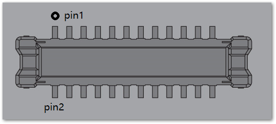 Figure 1: WisBlock 24-pin module connector
Pinout definition for standard size slot (A-D):
| D | C | B | A | Pin Number | Pin Number | A | B | C | D |
|---|---|---|---|---|---|---|---|---|---|
| NC | NC | NC | TXD0 | 1 | 2 | GND | GND | GND | GND |
| SPI_CS | SPI_CS | SPI_CS | SPI_CS | 3 | 4 | SPI_CLK | SPI_CLK | SPI_CLK | SPI_CLK |
| SPI_MISO | SPI_MISO | SPI_MISO | SPI_MISO | 5 | 6 | SPI_MOSI | SPI_MOSI | SPI_MOSI | SPI_MOSI |
| I2C1_SCL | I2C1_SCL | I2C1_SCL | I2C1_SCL | 7 | 8 | I2C1_SDA | I2C1_SDA | I2C1_SDA | I2C1_SDA |
| VDD | VDD | VDD | VDD | 9 | 10 | IO2 | IO1 | IO4 | IO6 |
| 3V3_S | 3V3_S | 3V3_S | 3V3_S | 11 | 12 | IO1 | IO2 | IO3 | IO5 |
| NC | NC | NC | NC | 13 | 14 | 3V3_S | 3V3_S | 3V3_S | 3V3_S |
| NC | NC | NC | NC | 15 | 16 | VDD | VDD | VDD | VDD |
| NC | NC | NC | NC | 17 | 18 | NC | NC | NC | NC |
| NC | NC | NC | NC | 19 | 20 | NC | NC | NC | NC |
| NC | NC | NC | NC | 21 | 22 | NC | NC | NC | NC |
| GND | GND | GND | GND | 23 | 24 | RXD0 | NC | NC | NC |
Pinout definition for double size sensor slot (E and F):
| Connector F | Connector E | Pin Number | Pin Number | Connector E | Connector F |
|---|---|---|---|---|---|
| TXD1 | TXD0 | 1 | 2 | GND | GND |
| SPI_CS | SPI_CS | 3 | 4 | SPI_CLK | SPI_CLK |
| SPI_MISO | SPI_MISO | 5 | 6 | SPI_MOSI | SPI_MOSI |
| I2C1_SCL | I2C1_SCL | 7 | 8 | I2C1_SDA | I2C1_SDA |
| VDD | VDD | 9 | 10 | IO3 | IO5 |
| 3V3_S | 3V3_S | 11 | 12 | IO4 | IO6 |
| NC | NC | 13 | 14 | 3V3_S | 3V3_S |
| NC | NC | 15 | 16 | VDD | VDD |
| NC | NC | 17 | 18 | NC | NC |
| NC | NC | 19 | 20 | NC | NC |
| NC | NC | 21 | 22 | NC | NC |
| GND | GND | 23 | 24 | RXD0 | RXD1 |
As for the following table, it shows the pin name and description of each pin in the 24-pin WisBlock module connector.
| Pin Number | Pin Name | Type | Description |
|---|---|---|---|
| 1 | TXD1 | I/O | UART TX signal |
| 2 | GND | S | Ground |
| 3 | SPI_CS | I/O | SPI chip select signal |
| 4 | SPI_CLK | I/O | SPI clock signal |
| 5 | SPI_MISO | I/O | SPI MISO signal |
| 6 | SPI_MOSI | I/O | SPI MOSI signal |
| 7 | I2C1_SCL | I/O | I2C clock signal |
| 8 | I2C1_SDA | I/O | I2C data signal |
| 9 | VDD | S | Generated by CPU module. Used to power sensor board if MCU IO level is not 3.3 V |
| 10 | IOx | I/O | General purpose IO pin. When 3V3_S is used, this pin cannot be used as an interrupt input. |
| 11 | 3V3_S | S | 3.3 V power supply. This power pin is controlled by IO2 from the WisBlock Core module. |
| 12 | IOx | I/O | General purpose IO pin. When 3V3_S is used, this pin cannot be used as an interrupt input. |
| 13 | NC | NC | Not connected |
| 14 | 3V3_S | S | 3.3 V power supply. This power pin is controlled by IO2 from the WisBlock Core module. |
| 15 | NC | NC | Not connected |
| 16 | VDD | S | Generated by CPU module. Used to power sensor board if the MCU IO level is not 3.3 V. |
| 17 | NC | NC | Not connected |
| 18 | NC | NC | Not connected |
| 19 | NC | NC | Not connected |
| 20 | NC | NC | Not connected |
| 21 | NC | NC | Not connected |
| 22 | NC | NC | Not connected |
| 23 | GND | S | Ground |
| 24 | RXD1 | I/O | UART RX signal |
Connector for WisBlock IO Slot
The WisBlock Module IO Slot connector, as shown in Figure 13, is a 40-pin board-to-board connector.
The two WisBlock 40-pin connectors have the same connections for all IO, signal, and serial pins (UART, SPI, I2C).
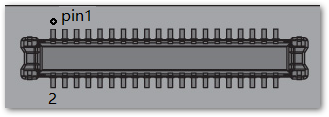 Figure 1: WisBlock IO slot connector
Pinout definition for IO slot:
| Connector B | Connector A | Pin Number | Pin Number | Connector A | Connector B |
|---|---|---|---|---|---|
| VBAT | VBAT | 1 | 2 | VBAT | VBAT |
| GND | GND | 3 | 4 | GND | GND |
| 3V3 | 3V3 | 5 | 6 | 3V3_S | 3V3_S |
| USB+ | USB+ | 7 | 8 | USB– | USB– |
| VBUS | VBUS | 9 | 10 | SW1 | SW1 |
| TXD0 | TXD0 | 11 | 12 | RXD0 | RXD0 |
| RESET | RESET | 13 | 14 | LED1 | LED1 |
| LED2 | LED2 | 15 | 16 | LED3 | LED3 |
| VDD | VDD | 17 | 18 | VDD | VDD |
| I2C1_SDA | I2C1_SDA | 19 | 20 | I2C1_SCL | I2C1_SCL |
| AIN0 | AIN0 | 21 | 22 | AIN1 | AIN1 |
| NC | NC | 23 | 24 | NC | NC |
| SPI_CS | SPI_CS | 25 | 26 | SPI_CLK | SPI_CLK |
| SPI_MISO | SPI_MISO | 27 | 28 | SPI_MOSI | SPI_MOSI |
| IO1 | IO1 | 29 | 30 | IO2 | IO2 |
| IO3 | IO3 | 31 | 32 | IO4 | IO4 |
| TXD1 | TXD1 | 33 | 34 | RXD1 | RXD1 |
| I2C2_SDA | I2C2_SDA | 35 | 36 | I2C2_SCL | I2C2_SCL |
| IO5 | IO5 | 37 | 38 | IO6 | IO6 |
| GND | GND | 39 | 40 | GND | GND |
As for the following table, it shows the pin name and description of the WisBlock IO module connector.
| Pin Number | Pin Name | Type | Description |
|---|---|---|---|
| 1 | VBAT | S | Power supply from battery |
| 2 | VBAT | S | Power supply from battery |
| 3 | GND | S | Ground |
| 4 | GND | S | Ground |
| 5 | 3V3 | S | 3.3 V power supply |
| 6 | 3V3_S | S | 3.3 V power supply. Can be shut down by a CPU module. |
| 7 | USB+ | I/O | USB D+ |
| 8 | USB– | I/O | USB D– |
| 9 | VBUS | S | 5 V input for USB |
| 10 | SW1 | I/O | User Defined Button (available on RAK4631/RAK4631-R and 11200 WisBlock Cores) |
| 11 | TXD0 | I/O | MCU UART0 TX signal |
| 12 | RXD0 | I/O | MCU UART0 RX signal |
| 13 | RESET | I | Connected to the reset switch, for MCU reset |
| 14 | LED1 | I/O | LED for battery charge indicator |
| 15 | LED2 | I/O | LED for custom used |
| 16 | LED3 | I/O | LED for custom used |
| 17 | VDD | S | Generated by CPU module - Used for power sensor board if the MCU IO level is not 3.3 V |
| 18 | VDD | S | Generated by CPU module - Used for power sensor board if the MCU IO level is not 3.3 V. |
| 19 | I2C1_SDA | I/O | The first set of I2C data signal |
| 20 | I2C1_SCL | I/O | The first set of I2C clock signal |
| 21 | AIN0 | A | Analog input for ADC |
| 22 | AIN1 | A | Analog input for ADC |
| 23 | NC | NC | Not connect |
| 24 | NC | NC | Not connect |
| 25 | SPI_CS | I/O | SPI chip select signal |
| 26 | SP_CLK | I/O | SPI clock |
| 27 | SPI_MISO | I/O | SPI MISO signal |
| 28 | SPI_MOSI | I/O | SPI MOSI signal |
| 29 | IO1 | I/O | General purpose IO |
| 30 | IO2 | I/O | Used for 3V3_S enable |
| 31 | IO3 | I/O | General purpose IO |
| 32 | IO4 | I/O | General purpose IO |
| 33 | TXD1 | I/O | MCU UART1 TX signal |
| 34 | RXD1 | I/O | MCU UART1 RX signal |
| 35 | I2C2_SDA | I/O | The second set of I2C data signal |
| 36 | I2C2_SCL | I/O | The second set of I2C clock signal |
| 37 | IO5 | I/O | General purpose IO |
| 38 | IO6 | I/O | General purpose IO |
| 39 | GND | S | Ground |
| 40 | GND | S | Ground |
Electrical Characteristics
Absolute Maximum Ratings
The Absolute Maximum Ratings of the device are shown in the table below. The stress ratings are the functional operation of the device.
- If the stress rating goes above what is listed, it may cause permanent damage to the device.
- Exposure to maximum rating conditions may affect the device reliability.
| Ratings | Maximum Value | Unit |
|---|---|---|
| Power Supply on the USB port (VBUS) | –0.3 to 5.5 | V |
| Battery Voltage (VBAT) | –0.3 to 4.3 | V |
| Solar Panel Voltage (CONN_S) | –0.3 to 5.5 | V |
| IOs of WisConnector | –0.3 to VDD+0.3 | V |
| ESD | 2000 | V |
The RAK19001, as any electronic equipment, is sensitive to electrostatic discharge (ESD). Improper handling can cause permanent damage to the module.
Current Consumption
The RAK19001 is designed for low-power IoT products. Its power supply uses a high-efficiency low ground current regulator. When there is no module on RAK19001, the leakage current is lower than 2 µA. With WisBlock Core and WisBlock sensor on it, the sleep current is lower than 10 µA. When a LoRa module is transmitting, the current may reach 130 mA.
| Conditions | Current | Unit |
|---|---|---|
| Leakage current, without any module on RAK19001 | 2 | µA |
| Idle current, with WisBlock Core and WisBlock Modules in sleep mode | 10 | µA |
| Working current, with LoRa module transmitting | 130 | mA |
Rechargeable Battery Connector
The RAK19001 WisBlock Base Board can be powered by a rechargeable battery connected to the P1 connector. The nominal operating voltage of the battery should be within the range shown in the following table. The matching connector for the battery wires is an JST PHR-2 2 mm pitch female
| Minimum | Typical | Maximum | Unit |
|---|---|---|---|
| 3.3 | 3.7 | 4.3 | V |
If a rechargeable battery is used, the USB connector is used as a charging port. The voltage and current fed to the battery through the port should not exceed its charging limits, as shown in the table below.
| Parameter | Value |
|---|---|
| Charging Voltage | 4.5 – 5.5 V |
| Charging Current | 500 mA |
A suitable Li-Ion battery should have the following parameters as shown in the table below:
| Parameter | Value |
|---|---|
| Standard Voltage | 3.7 V |
| Charging Voltage | 4.2 V |
| Capacity | As required |
| Discharge current | At least 500 mA |
Non-Rechargeable Battery Connector
The RAK19001 WisBlock Base Board can be powered by a Non-rechargeable battery connected to the P3 connector. The nominal operating voltage of the battery should be within the range shown in the following table. The matching connector for the battery wires is an
| Minimum | Typical | Maximum | Unit |
|---|---|---|---|
| 3.3 | 3.7 | 5.5 | V |
Solar Panel Connector
A 5 V solar panel can be connected to the board via the P2 connector to also serve the purpose of charging the battery. The matching connector for the solar panel wires is an JST ZHR-2 1.5 mm pitch female
Mechanical Characteristics
Board Dimensions
You may also refer and download the M1.2 Stand-off fastener/inserts datasheet.
Figure 14 shows the detailed mechanical dimensions of RAK19001.
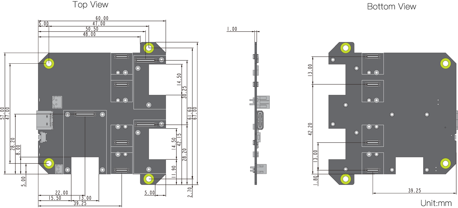 Figure 1: RAK19001 board dimensions
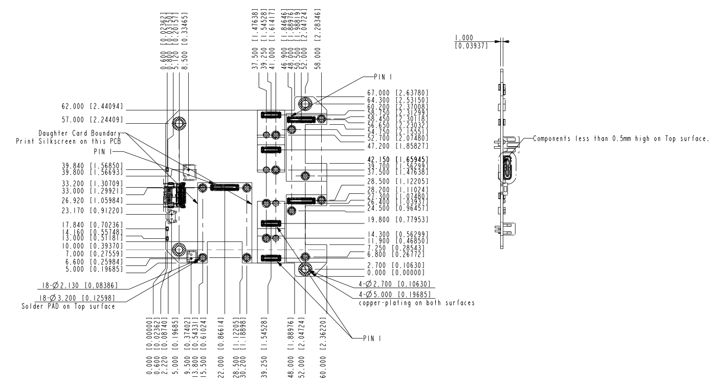 Figure 1: RAK19001 mechanical dimensions
WisConnector PCB Layout
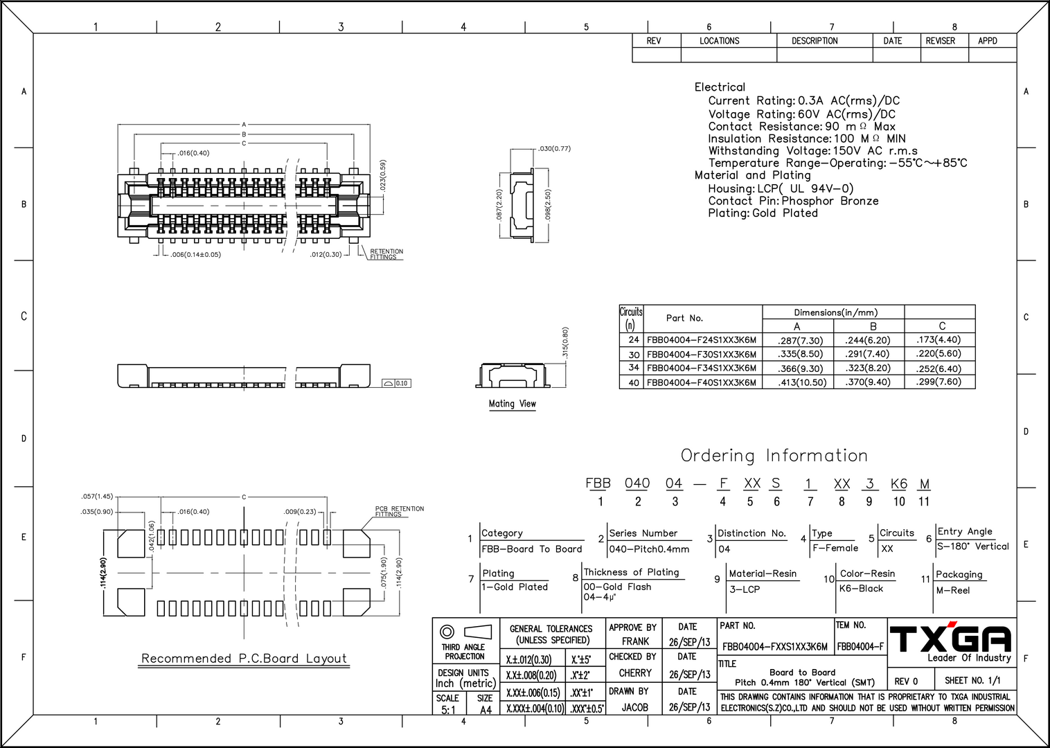 Figure 1: WisConnector PCB footprint and recommendations
Environmental Characteristics
The table below lists the operation and storage temperature requirements of RAK19001:
| Parameter | Minimum | Typical | Maximum |
|---|---|---|---|
| Operational Temperature Range | –35 ºC | +25 ºC | +75 ºC |
| Extended Temperature Range | –40 ºC | +25 ºC | +80 ºC |
| Storage Temperature Range | –40 ºC | +25 ºC | +80 ºC |
Schematic Diagram
The component schematics diagram of the RAK19001 are shown in Figure 14 and Figure 15.
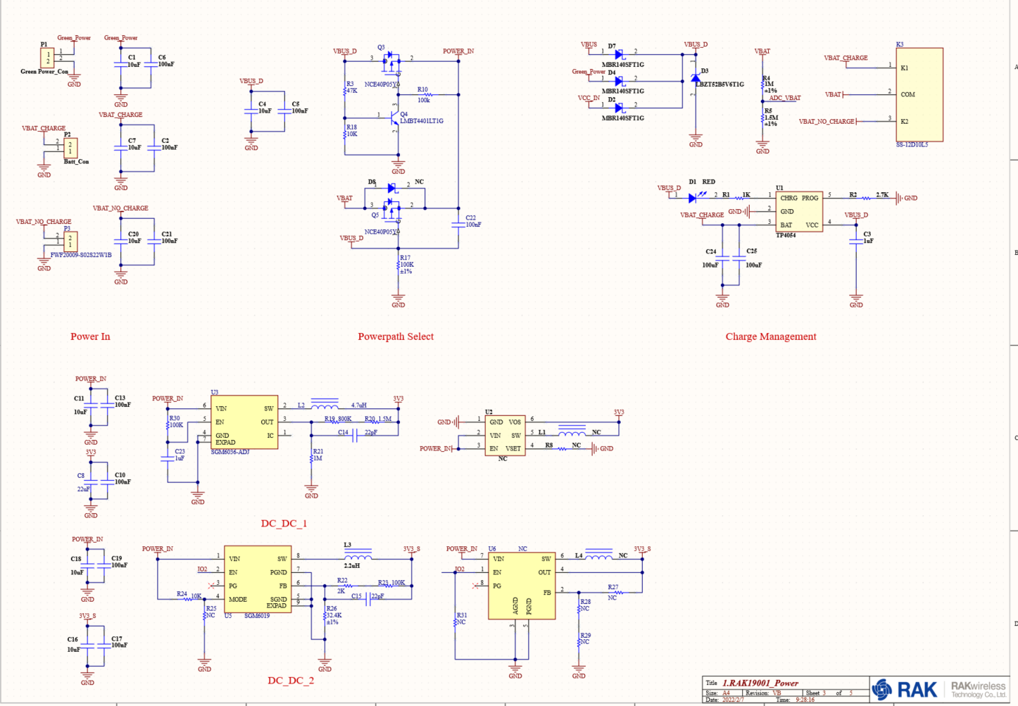 Figure 1: RAK19001 schematic diagram
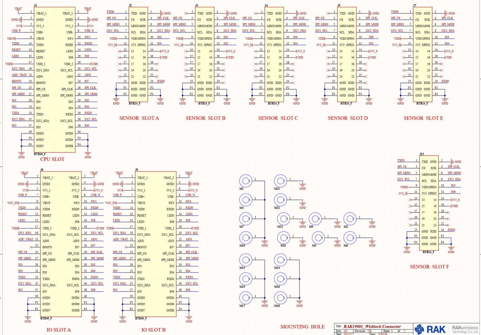 Figure 1: RAK19001 schematic diagram
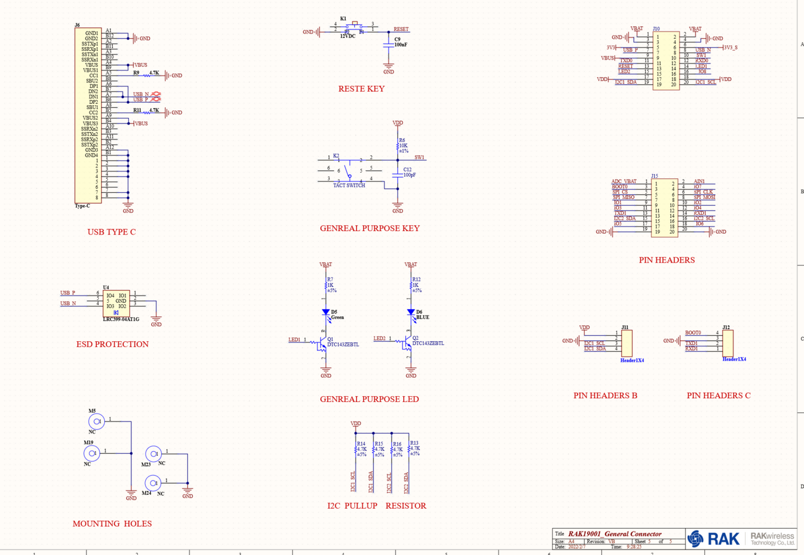 Figure 1: RAK19001 schematic diagram (Connectors)