RAK19010 WisBlock Base Board with Power Slot Datasheet
Overview
Description
RAK19010 is a WisBlock Base Board with Power Slot that connects WisBlock Core and other WisBlock Modules. The power slot of RAK19010 is required to have an attached WisBlock Power Slot module that provides power supply to the core and other modules. There are many different types of power slot modules compatible with RAK19010 and the choice will depend on the type of application.
It has one slot reserved for the power slot module, one for the core module, one slot for the IO module, and four sensor slots A-D for small WisBlock modules. The WisBlock Core, Power, and IO modules are attached on the top side, and smaller WisBlock modules can be attached to the top or bottom side of the RAK19010. Slot A and D hold modules up to 23 mm in size, while all slots A up to D support 10 mm WisBlock modules. Also, there are three 2.54 mm pitch headers for extension interface with BOOT, GPIO, ADC, I2C, and UART pins.
WisBlock modules are connected to the RAK19010 WisBlock Base board via high-speed board-to-board connectors. They provide secure and reliable interconnection to ensure the signal integrity of each data bus. A set of screws is used to fix the modules, making it reliable even in an environment with lots of vibrations.
You can also use a RAK19005 WisBlock Sensor Extension Cable or RAK19008 WisBlock IO Extension Cable to position the WisBlock modules apart from the WisBlock Base board or in any part of your case.
Applications
- Wireless sensor network
- Environmental monitoring
- Wireless data transmission
- Data acquisition in the industrial environment
- Location and tracking of personnel or moving objects
Features
- Flexible building block design, which enables modular function realization and expansion
- High-speed interconnection secured with screws to ensure signal integrity
- Supports multiple types of low-power MCUs
- Supports multiple types of sensors - a single board can support a combination of two different types of sensors
- Supports different power modules depending on the applications.
- RAK19012 - USB, LiPo and Solar
- RAK19013 - LiPo and Solar
- RAK19015 - Battery
- RAK19016 - 5 V to 24 V voltage input
- Module Slots
- 1 WisBlock Core module
- 1 WisBlock power module
- 1 WisBlock module compatible with IO slot
- 4 WisBlock modules compatible with slots A-D
- Pin headers accessible pins for BOOT, GPIO, ADC, I2C, and UART interfaces
- Size
- RAK19010 has a size of only 30 x 60 mm, which lets you create solutions that fit into the smallest housings.
If you can't find a WisBlock module that fits your IoT requirements, use the standard connectors of WisBlock to develop your specific function module. WisBlock supports open-source hardware architecture and you can find tutorials showing how to create your own Awesome WisBlock module.
Specifications
Block Overview
There are seven (7) slots on RAK19010 WisBlock Base Board with Power Slot:
- CPU SLOT: This slot is reserved for the WisBlock Core module which has the main MCU.
- Power SLOT: This slot is required to provide power to WisBlock Core and modules.
- IO SLOT: This slot is used for IO extension modules.
- Four Sensor Slots: The sensor slots A to D are used to connect with the I2C bus. Slots A and D can be used for GNSS modules, too.
Also, there are pin headers 2.54 mm pitch for the extension interface that connects to BOOT, I2C, UART, ADC, and GPIO pins.
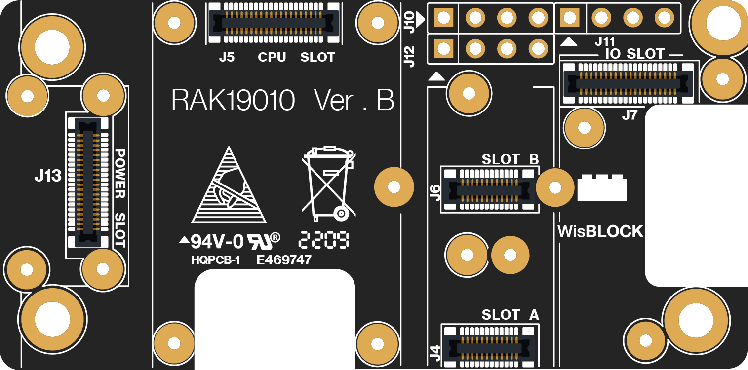 Figure 1: RAK19010 WisBlock Base Board with Power Slot top view
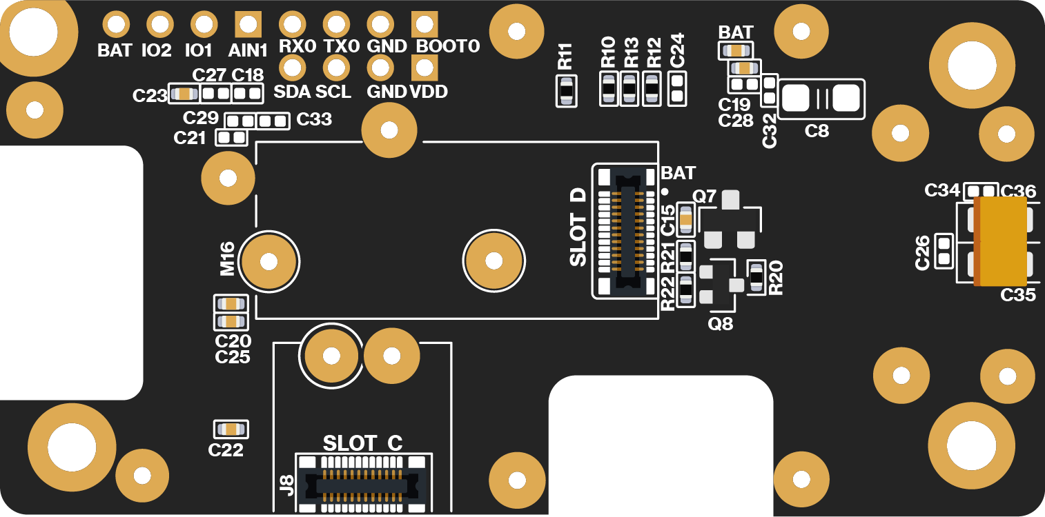 Figure 1: RAK19010 WisBlock Base Board with Power Slot bottom view
Block Diagram
The block diagram in Figure 3 shows the internal architecture and external interfaces of the RAK19010 board.
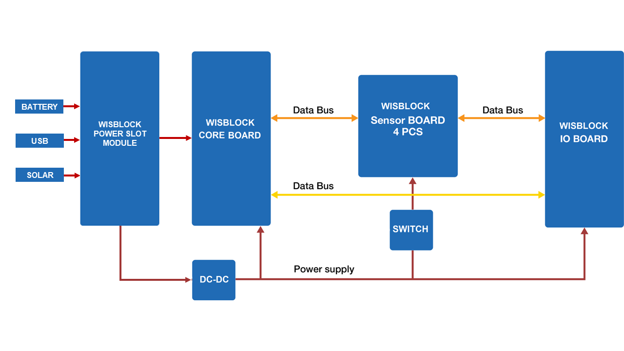 Figure 1: RAK19010 WisBlock Base Board wth Power Slot block diagram
Hardware
The hardware specification is categorized into six parts. It shows the interfacing, pinouts, and their corresponding functions and diagrams. It also presents the electrical, environmental, and mechanical parameters that include the tabular data of the functionalities and standard values of the RAK19010 WisBlock Base Board 2nd Gen.
Interfaces
RAK19010 WisBlock Base Board with Power Slot provides the following interfaces, headers, a button, and WisBlock Connectors.
- One connector for CPU slot
- One connector for the power slot
- One connector for the IO slot
- Four connectors for WisBlock sensor modules (slots A to D)
- Three 4-pin header 2.54 mm hole pads (GPIO, ADC, UART, I2C, Power)
Figure 4 show the location of RAK19010 main components.
 Figure 1: RAK19010 top and bottom parts
J10, J11, J12 Headers
On the RAK19010 Base Board, there are three 2.54 mm pitch headers for IO extension. BOOT, I2C, GPIO, and UART pins from the WisBlock Core module are also connected to these headers.
J10 Header Pinout
| Pin | Pin Name | Description |
|---|---|---|
| 1 | BOOT | MCU BOOT pin |
| 2 | GND | Ground pin |
| 3 | TX1 | UART1 TX pin |
| 4 | RX1 | UART1 RX pin |
J11 Header Pinout
| Pin | Pin Name | Description |
|---|---|---|
| 1 | AIN1 | ADC input signal |
| 2 | IO1 | General purpose IO |
| 3 | IO2 | General purpose IO |
| 4 | VBAT | Battery voltage |
J12 Header Pinout
| Pin | Pin Name | Description |
|---|---|---|
| 1 | VDD | 3.3 V |
| 2 | GND | Ground pin |
| 3 | SCL | I2C1 clock |
| 4 | SDA | I2C2 data |
BOOT pin is used on startup configuration or sequence of the WisBlock Core connected to it. It is commonly used for uploading the bootloader and/or application firmware. The requirements of the state of the BOOT pin depend on the specific model of the WisBlock Core used.
Pin Definition
Connector for WisBlock Core
The WisBlock Core module connector is a 40-pin board-to-board connector. It is a high-speed and high-density connector, with an easy attaching mechanism.
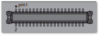 Figure 1: WisBlock Core module connector
The table below shows the pinout of the 40-pin WisBlock core connector:
| Function Name of WisBlock Base | Pin Number | Pin Number | Function Name of WisBlock Base |
|---|---|---|---|
| VBAT | 1 | 2 | VBAT |
| GND | 3 | 4 | GND |
| 3V3 | 5 | 6 | 3V3 |
| USB+ | 7 | 8 | USB– |
| VBUS | 9 | 10 | SW1 |
| TXD0 | 11 | 12 | RXD0 |
| RESET | 13 | 14 | LED1 |
| LED2 | 15 | 16 | LED3 |
| VDD | 17 | 18 | VDD |
| I2C1_SDA | 19 | 20 | I2C1_SCL |
| AIN0 | 21 | 22 | AIN1 |
| BOOT0 | 23 | 24 | IO7 |
| SPI_CS | 25 | 26 | SPI_CLK |
| SPI_MIS0 | 27 | 28 | SPI_MOSI |
| IO1 | 29 | 30 | IO2 |
| IO3 | 31 | 32 | IO4 |
| TXD1 | 33 | 34 | RXD1 |
| I2C2_SDA | 35 | 36 | I2C2_SCL |
| IO5 | 37 | 38 | IO6 |
| GND | 39 | 40 | GND |
As for the following table, it shows the definition of each pin of the WisBlock Core connector:
| Pin Number | Pin Name | Type | Description |
|---|---|---|---|
| 1 | VBAT | S | Power supply from battery |
| 2 | VBAT | S | Power supply from battery |
| 3 | GND | S | Ground |
| 4 | GND | S | Ground |
| 5 | 3V3 | S | 3.3 V power supply |
| 6 | 3V3 | S | 3.3 V power supply |
| 7 | USB+ | I/O | USB D+ |
| 8 | USB– | I/O | USB D– |
| 9 | VBUS | S | VBUS for USB |
| 10 | SW1 | I/O | Switch signal for customer's control |
| 11 | TXD0 | I/O | MCU UART0 TX signal |
| 12 | RXD0 | I/O | MCU UART0 RX signal |
| 13 | RESET | I | Connected to the reset switch, for MCU reset |
| 14 | LED1 | I/O | LED for battery charging indication |
| 15 | LED2 | I/O | LED for custom usage |
| 16 | LED3 | I/O | LED for custom usage |
| 17 | VDD | S | Generated by MCU module for power sensor board if the MCU IO level is not 3.3 V |
| 18 | VDD | S | Generated by MCU module for power sensor board if the MCU IO level is not 3.3 V |
| 19 | I2C1_SDA | I/O | The first set of I2C data signal |
| 20 | I2C1_SCL | I/O | The first set of I2C clock signals |
| 21 | AIN0 | A | Analog input for ADC |
| 22 | AIN1 | A | Analog input for ADC |
| 23 | BOOT0 | I | For ST MCU, set high when reset. The MCU will allow you to enter boot mode. |
| 24 | IO7 | I/O | Not connected |
| 25 | SPI_CS | I/O | SPI chip select signal |
| 26 | SPI_CLK | I/O | SPI clock |
| 27 | SPI_MISO | I/O | SPI MISO signal |
| 28 | SPI_MOSI | I/O | SPI MOSI signal |
| 29 | IO1 | I/O | General purpose IO |
| 30 | IO2 | I/O | Used for 3V3_S enable |
| 31 | IO3 | I/O | General purpose IO |
| 32 | IO4 | I/O | General purpose IO |
| 33 | TXD1 | I/O | MCU UART1 RX signal |
| 34 | RXD1 | I/O | MCU UART1 RX signal |
| 35 | I2C2_SDA | I/O | The second set of I2C data signal |
| 36 | I2C2_SCL | I/O | The second set of I2C data signal |
| 37 | IO5 | I/O | General purpose IO |
| 38 | IO6 | I/O | General purpose IO |
| 39 | GND | S | Ground |
| 40 | GND | S | Ground |
Connector for WisBlock Power
The WisPower module connector is a 40-pin board-to-board connector. It is a high-speed and high-density connector, with an easy attaching mechanism.
 Figure 1: WisBlock Power Slot module connector
The table below shows the pinout of the 40-pin power module connector:
| Pin Number | Function Name of WisBlock Base | Pin Number | Function Name of WisBlock Base |
|---|---|---|---|
| 1 | VBAT | 2 | VBAT |
| 3 | GND | 4 | GND |
| 5 | 3V3 | 6 | 3V3 |
| 7 | USB+ | 8 | USB– |
| 9 | VBUS | 10 | VBUS |
| 11 | NC | 12 | NC |
| 13 | RESET | 14 | LED1 |
| 15 | LED2 | 16 | NC |
| 17 | 3V3 | 18 | 3V3 |
| 19 | I2C1_SDA | 20 | I2C1_SCL |
| 21 | AIN0 | 22 | AIN1 |
| 23 | NC | 24 | NC |
| 25 | SPI_CS | 26 | SPI_CLK |
| 27 | SPI_MISO | 28 | SPI_MOSI |
| 29 | NC | 30 | NC |
| 31 | NC | 32 | NC |
| 33 | NC | 34 | NC |
| 35 | I2C2_SDA | 36 | I2C2_SCL |
| 37 | IO5 | 38 | IO6 |
| 39 | GND | 40 | GND |
As for the following table, it shows the definition of each pin of the WisBlock Power connector:
| Pin Number | Pin Name | Type | Description |
|---|---|---|---|
| 1 | VBAT | S | Power supply from battery |
| 2 | VBAT | S | Power supply from battery |
| 3 | GND | S | Ground |
| 4 | GND | S | Ground |
| 5 | 3V3 | S | 3.3 V power supply |
| 6 | 3V3 | S | 3.3 V power supply |
| 7 | USB+ | I/O | USB D+ |
| 8 | USB– | I/O | USB D– |
| 9 | VBUS | S | USB VBUS |
| 10 | VBUS | S | USB VBUS |
| 11 | NC | NC | Not connected |
| 12 | NC | NC | Not connected |
| 13 | RESET | I | Connected to the reset switch, for MCU reset |
| 14 | LED1 | I/O | LED for battery charging indication |
| 15 | LED2 | I/O | LED for custom usage |
| 16 | NC | NC | Not connected |
| 17 | 3V3 | S | 3.3 V power supply |
| 18 | 3V3 | S | 3.3 V power supply |
| 19 | I2C1_SDA | I/O | The first set of I2C data signal |
| 20 | I2C1_SCL | I/O | The first set of I2C clock signal |
| 21 | AIN0 | A | Analog input for ADC |
| 22 | AIN1 | A | Analog input for ADC |
| 23 | NC | NC | Not connected |
| 24 | NC | NC | Not connected |
| 25 | SPI_CS | I/O | SPI chip select signal |
| 26 | SPI_CLK | I/O | SPI clock signal |
| 27 | SPI_MISO | I/O | SPI MISO signal |
| 28 | SPI_MOSI | I/O | SPI MOSI signal |
| 29 | NC | NC | Not connected |
| 30 | NC | NC | Not connected |
| 31 | NC | NC | Not connected |
| 32 | NC | NC | Not connected |
| 33 | NC | NC | Not connected |
| 34 | NC | NC | Not connected |
| 35 | I2C2_SDA | I/O | The second set of I2C data signal |
| 36 | I2C2_SCL | I/O | The second set of I2C clock signal |
| 37 | IO5 | I/O | General purpose IO |
| 38 | IO6 | I/O | General purpose IO |
| 39 | GND | S | Ground |
| 40 | GND | S | Ground |
Connectors for WisBlock Sensor
The WisBlock sensor module connector is a 24-pin board-to-board connector.
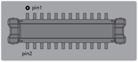 Figure 1: WisBlock Sensor module connector
There are four connectors reserved for the sensor modules on the RAK19010. The pinout definition of the WisBlock modules with a 24-pin connector on WisBlock Base Board varies according to its connector.
| Connector D | Connector C | Connector B | Connector A | Pin Number | Pin Number | Connector A | Connector B | Connector C | Connector D |
|---|---|---|---|---|---|---|---|---|---|
| TXD1 | NC | NC | TXD1 | 1 | 2 | GND | GND | GND | GND |
| SPI_CS | SPI_CS | SPI_CS | SPI_CS | 3 | 4 | SPI_CLK | SPI_CLK | SPI_CLK | SPI_CLK |
| SPI_MISO | SPI_MISO | SPI_MISO | SPI_MISO | 5 | 6 | SPI_MOSI | SPI_MOSI | SPI_MOSI | SPI_MOSI |
| I2C1_SCL | I2C1_SCL | I2C1_SCL | I2C1_SCL | 7 | 8 | I2C1_SDA | I2C1_SDA | I2C1_SDA | I2C1_SDA |
| VDD | VDD | VDD | VDD | 9 | 10 | IO2 | IO1 | IO4 | IO6 |
| 3V3_S | 3V3_S | 3V3_S | 3V3_S | 11 | 12 | IO1 | IO2 | IO3 | IO5 |
| NC | NC | NC | NC | 13 | 14 | 3V3_S | 3V3_S | 3V3_S | 3V3_S |
| NC | NC | NC | NC | 15 | 16 | VDD | VDD | VDD | VDD |
| NC | NC | NC | NC | 17 | 18 | NC | NC | NC | NC |
| NC | NC | NC | NC | 19 | 20 | NC | NC | NC | NC |
| NC | NC | NC | NC | 21 | 22 | NC | NC | NC | NC |
| GND | GND | GND | GND | 23 | 24 | RXD1 | NC | NC | RXD1 |
As for the following table, it shows the pin name and description of each pin in the WisBlock Sensor module connector.
| Pin Number | Connector A | Connector B | Connector C | Connector D | Type | Description |
|---|---|---|---|---|---|---|
| 1 | TXD1 | NC | NC | TXD1 | I/O | UART TX signal |
| 2 | GND | GND | GND | GND | S | Ground |
| 3 | SPI_CS | SPI_CS | SPI_CS | SPI_CS | I/O | SPI chip select signal |
| 4 | SPI_CLK | SPI_CLK | SPI_CLK | SPI_CLK | I/O | SPI clock |
| 5 | SPI_MISO | SPI_MISO | SPI_MISO | SPI_MISO | I/O | SPI MISO signal |
| 6 | SPI_MOSI | SPI_MOSI | SPI_MOSI | SPI_MOSI | I/O | SPI MOSI signal |
| 7 | I2C1_SCL | I2C1_SCL | I2C1_SCL | I2C1_SCL | I/O | I2C clock signal |
| 8 | I2C1_SDA | I2C1_SDA | I2C1_SDA | I2C1_SDA | I/O | I2C data signal |
| 9 | VDD | VDD | VDD | VDD | S | Generated by CPU module. Used to power sensor board if MCU IO level is not 3.3 V |
| 10 | IO2 | IO1 | IO4 | IO6 | I/O | General purpose IO. IO2 controls the power switch of 3V3_S. When the 3V3_S function is used, IO2 can not be used as an interrupt of the sensor. |
| 11 | 3V3_S | 3V3_S | 3V3_S | 3V3_S | S | 3.3 V power supply. Can be shut down by the CPU module. |
| 12 | IO1 | IO2 | IO3 | IO5 | I/O | General purpose IO - IO controls the power switch of 3V3_S. When the 3V3_S function is used, IO2 cannot be used as an interrupt of the sensor. |
| 13 | NC | NC | NC | NC | NC | Not connected |
| 14 | 3V3_S | 3V3_S | 3V3_S | 3V3_S | S | 3.3 V power supply. Can be shut down by the CPU module. |
| 15 | NC | NC | NC | NC | NC | Not connected |
| 16 | VDD | VDD | VDD | VDD | S | Generated by CPU module. Used to power sensor board if the MCU IO level is not 3.3 V. |
| 17 | NC | NC | NC | NC | NC | Not connected |
| 18 | NC | NC | NC | NC | NC | Not connected |
| 19 | NC | NC | NC | NC | NC | Not connected |
| 20 | NC | NC | NC | NC | NC | Not connected |
| 21 | NC | NC | NC | NC | NC | Not connected |
| 22 | NC | NC | NC | NC | NC | Not connected |
| 23 | GND | GND | GND | GND | S | Ground |
| 24 | RXD1 | NC | NC | RXD1 | I/O | UART RX signal |
Connector for WisBlock IO Slot
The WisBlock Module IO Slot connector, as shown in Figure 8, is a 40-pin board-to-board connector.
 Figure 1: WisBlock IO slot connector
Pinout definition for IO slot:
| Connector B | Connector A | Pin Number | Pin Number | Connector A | Connector B |
|---|---|---|---|---|---|
| VBAT | VBAT | 1 | 2 | VBAT | VBAT |
| GND | GND | 3 | 4 | GND | GND |
| 3V3 | 3V3 | 5 | 6 | 3V3_S | 3V3_S |
| USB+ | USB+ | 7 | 8 | USB– | USB– |
| VBUS | VBUS | 9 | 10 | SW1 | SW1 |
| TXD0 | TXD0 | 11 | 12 | RXD0 | RXD0 |
| RESET | RESET | 13 | 14 | LED1 | LED1 |
| LED2 | LED2 | 15 | 16 | LED3 | LED3 |
| VDD | VDD | 17 | 18 | VDD | VDD |
| I2C1_SDA | I2C1_SDA | 19 | 20 | I2C1_SCL | I2C1_SCL |
| AIN0 | AIN0 | 21 | 22 | AIN1 | AIN1 |
| NC | NC | 23 | 24 | NC | NC |
| SPI_CS | SPI_CS | 25 | 26 | SPI_CLK | SPI_CLK |
| SPI_MISO | SPI_MISO | 27 | 28 | SPI_MOSI | SPI_MOSI |
| IO1 | IO1 | 29 | 30 | IO2 | IO2 |
| IO3 | IO3 | 31 | 32 | IO4 | IO4 |
| TXD1 | TXD1 | 33 | 34 | RXD1 | RXD1 |
| I2C2_SDA | I2C2_SDA | 35 | 36 | I2C2_SCL | I2C2_SCL |
| IO5 | IO5 | 37 | 38 | IO6 | IO6 |
| GND | GND | 39 | 40 | GND | GND |
As for the following table, it shows the pin name and description of the WisBlock IO module connector.
| Pin Number | Pin Name | Type | Description |
|---|---|---|---|
| 1 | VBAT | S | Power supply from battery |
| 2 | VBAT | S | Power supply from battery |
| 3 | GND | S | Ground |
| 4 | GND | S | Ground |
| 5 | 3V3 | S | 3.3 V power supply |
| 6 | 3V3_S | S | 3.3 V power supply. Can be shut down by a CPU module. |
| 7 | USB+ | I/O | USB D+ |
| 8 | USB– | I/O | USB D– |
| 9 | VBUS | S | 5 V input for USB |
| 10 | SW1 | I/O | Switch signal for custom used |
| 11 | TXD0 | I/O | MCU UART0 TX signal |
| 12 | RXD0 | I/O | MCU UART0 RX signal |
| 13 | RESET | I | Connected to the reset switch, for MCU reset |
| 14 | LED1 | I/O | LED for battery charge indicator |
| 15 | LED2 | I/O | LED for custom used |
| 16 | LED3 | I/O | LED for custom used |
| 17 | VDD | S | Generated by CPU module - Used for power sensor board if the MCU IO level is not 3.3 V |
| 18 | VDD | S | Generated by CPU module - Used for power sensor board if the MCU IO level is not 3.3 V. |
| 19 | I2C1_SDA | I/O | The first set of I2C data signal |
| 20 | I2C1_SCL | I/O | The first set of I2C clock signals |
| 21 | AIN0 | A | Analog input for ADC |
| 22 | AIN1 | A | Analog input for ADC |
| 23 | NC | NC | Not connect |
| 24 | NC | NC | Not connect |
| 25 | SPI_CS | I/O | SPI chip select signal |
| 26 | SP_CLK | I/O | SPI clock |
| 27 | SPI_MISO | I/O | SPI MISO signal |
| 28 | SPI_MOSI | I/O | SPI MOSI signal |
| 29 | IO1 | I/O | General purpose IO |
| 30 | IO2 | I/O | Used for 3V3_S enable |
| 31 | IO3 | I/O | General purpose IO |
| 32 | IO4 | I/O | General purpose IO |
| 33 | TXD1 | I/O | MCU UART1 TX signal |
| 34 | RXD1 | I/O | MCU UART1 RX signal |
| 35 | I2C2_SDA | I/O | The second set of I2C data signal |
| 36 | I2C2_SCL | I/O | The second set of I2C clock signal |
| 37 | IO5 | I/O | General purpose IO |
| 38 | IO6 | I/O | General purpose IO |
| 39 | GND | S | Ground |
| 40 | GND | S | Ground |
Electrical Characteristics
Absolute Maximum Ratings
The Absolute Maximum Ratings of the device are shown in the table below. The stress ratings are the functional operation of the device.
- If the stress rating goes above what is listed, it may cause permanent damage to the device.
- Under the listed conditions is not advised.
- Exposure to maximum rating conditions may affect the device reliability.
| Ratings | Maximum Value | Unit |
|---|---|---|
| IOs of WisConnector | –0.3 to VDD+0.3 | V |
| ESD | 2000 | V |
The RAK19010, like any electronic equipment, is sensitive to electrostatic discharge (ESD). Improper handling can cause permanent damage to the module.
Mechanical Characteristics
Board Dimensions
You may also refer and download the M1.2 Stand-off fastener/inserts datasheet.
Figure 9 shows the detailed mechanical dimensions of the RAK19010 Board.
 Figure 1: RAK19010 mechanical board dimension
Figure 10 shows the mounting holes location and diameter of the RAK19010 Board.
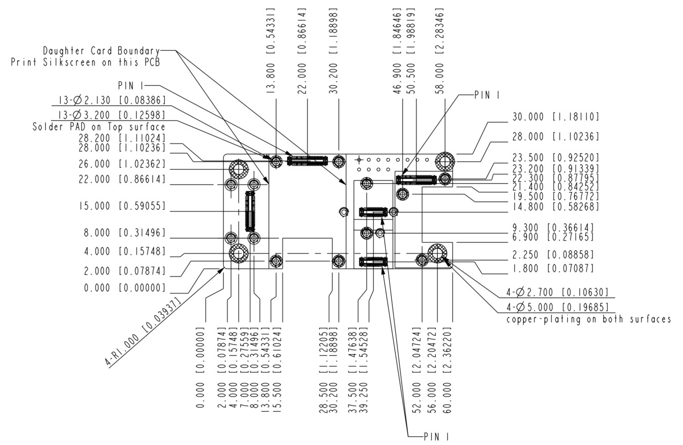 Figure 1: RAK19010 mechanical dimensions and mounting holes locations
WisConnector PCB Layout
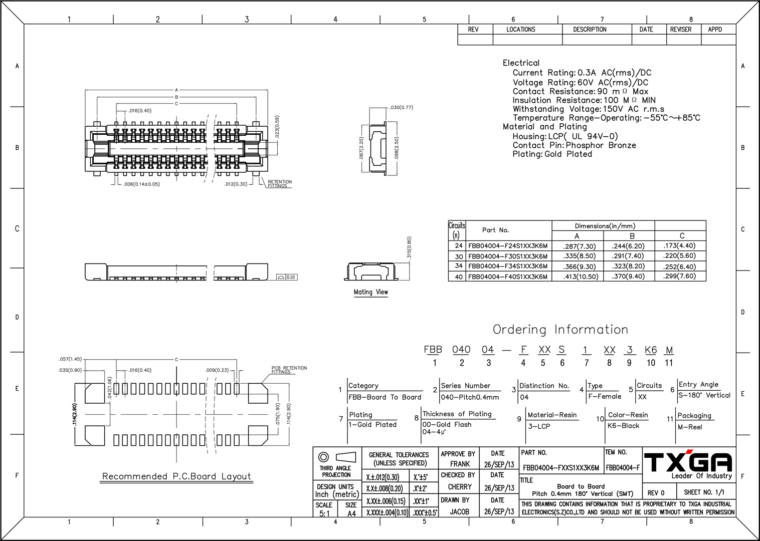 Figure 1: WisConnector PCB footprint and recommendations
Environmental Characteristics
The table below lists the operation and storage temperature requirements of RAK19010:
| Parameter | Minimum | Typical | Maximum |
|---|---|---|---|
| Operational temperature range | –35 ºC | +25 ºC | +75 ºC |
| Extended temperature range | –40 ºC | +25 ºC | +80 ºC |
| Storage temperature range | –40 ºC | +25 ºC | +80 ºC |
Schematic Diagram
The component schematics diagram of the RAK19010 is shown in Figure 12.
 Figure 1: RAK19010 schematic diagram (Power)