RAK3172-SiP WisDuo LPWAN SiP Datasheet
Overview
Description
RAK3172-SiP (and the RAK3172LP-SiP variant) are low-power, long-range transceivers based on the STM32WLE5JC SoC in a system-in-package form factor. These two modules use different RF output paths to optimize current consumption depending on the application. RAK3172-SiP uses RFO_HP, while RAK3172LP-SiP uses the RFO_LP of the STM32WL SoC transceiver.
WisDuo SiP LoRa modules provide a small, easy-to-use, low-power solution for long-range wireless data applications. These modules comply with Classes A, B, and C of the LoRaWAN 1.0.3 specifications. They can easily connect to different LoRaWAN server platforms such as TheThingsNetwork (TTN), Helium, ChirpStack, and Actility. They also support LoRa point-to-point (P2P) communication mode, which facilitates the quick implementation of customized long-range LoRa networks.
You can configure the mode and operation of the RAK3172-SiP/RAK3172LP-SiP using AT commands via a UART interface or create custom firmware using the RUI3 API. The RAK3172-SiP/RAK3172LP-SiP are very small and offer low-power features suitable for battery-powered applications.
The RAK3172-SiP does not have pre-flashed LoRaWAN credentials and you have to define and setup your own unique credentials for the SiP's.
Features
- Based on STM32WLE5JC
- Two variants available
- RAK3172-SiP (uses RFO_HP)
- RAK3172LP-SiP (uses RFO_LP)
- System-in-Package form factor
- RUI3 API compatible
- LoRaWAN 1.0.3 specification compliant
- Supported bands: IN865, EU868, AU915, US915, KR920, RU864, and AS923
- LoRaWAN Activation by OTAA/ABP
- LoRa Point-to-Point (P2P) communication
- Custom firmware using Arduino via RUI3 API
- Easy-to-use AT Command set via UART interface
- Long-range - up to 15 km with optimized antenna
- ARM Cortex-M4 32-bit
- 256 kbytes flash memory with ECC
- 64 kbytes RAM
- Ultra-low power consumption of 1.69 μA in sleep mode
- Supply voltage: 2.0 V ~ 3.6 V
- Temperature range: -40° C ~ 85° C
- Size: 12 mm x 12 mm x 1.22 mm
- Package: LGA73 type
Specifications
This section covers the hardware and software specifications for the RAK3172-SiP. It also includes a block diagram and an updated firmware link for the RAK3172-SiP WisDuo Module.
Overview
Block Diagram
 Figure 1: RAK3172-SiP system block diagram
Hardware
The hardware specification is categorized into six parts. It discusses the interfacing, pinouts, and their corresponding functions and diagrams. It also covers the RF, electrical, mechanical, and environmental parameters, including tabular data of the functionalities and standard values of the RAK3172-SiP WisDuo LPWAN SiP module.
For the reference application schematic of RAK3172-SiP with minimum components requirements, refer to the RAK3272-SiP Breakout Board Datasheet.
Interfaces
| Module | Interfaces |
|---|---|
| RAK3172-SiP | UART2 (Default for AT Command), UART1 |
| RAK3172LP-SiP | UART2 (Default for AT Command), UART1 |
Pin Definition
You can check the pin definitions on the table and illustration, as shown in Figure 2.
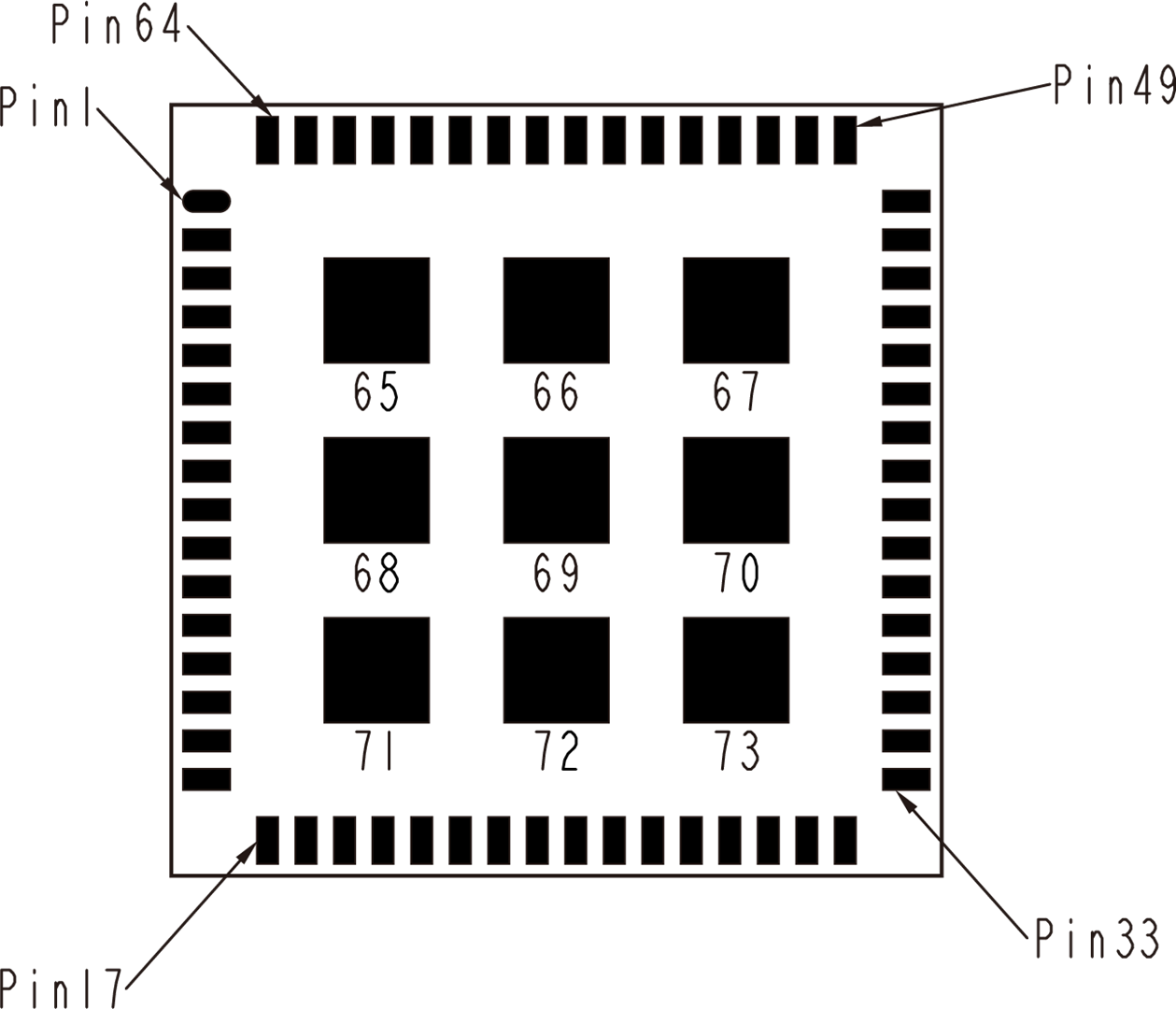 Figure 1: RAK3172-SiP top view pin diagram
When using the RF_OUT pin for an antenna and not the IPEX connector variant, design considerations are necessary to ensure optimum RF performance.
- The RF trace must be away from sources of interference (switching nodes of DC-DC supplies, high-current/high-voltage pulses from controllers of inductive loads like motors, signal generators, etc.).
- The RF trace must have 50-ohm impedance. Using impedance simulation software is advisable to achieve this.
- If using an external antenna connector, position it close to the
RF_OUTpin. - Ground plane optimization is critical for certain antenna types, such as monopoles.
- The GND trace used for the RF return path must be directly connected to the GND plane and not treated as a thermal relief.
- It is recommended to route the RF trace in a curve, rather than with sharp 90-degree angles.
In addition, with a commitment to making IoT easy, RAK offers a dedicated service for Antenna RF Design which includes PCB design, tuning, matching, and RF testing.
| Pin No. | Name | Type | Description |
|---|---|---|---|
| 1 | PA13 | I | Reserved - SWD debug pin (SWDIO) |
| 2 | PA14 | O | Reserved - SWD debug pin (SWCLK) |
| 3 | VDD | VDD | |
| 4 | VBAT | VDD (For RTC) | |
| 5 | PC13 | I/O | GPIO |
| 6 | VREF+ | Input reference voltage for ADC | |
| 7 | VDDA | External power supply for the analog sections (ADC Converter) | |
| 8 | PA15 | I/O | GPIO or PIN_A4 |
| 9 | PB15 | I/O | GPIO |
| 10 | VFBSMPS | DC-DC switching power feedback | |
| 11 | VDDMPS | DC-DC switching power input | |
| 12 | GND | Ground | |
| 13 | VLXSMPS | DC-DC switching output | |
| 14 | PB3 | I/O | GPIO or PIN_A0 |
| 15 | PB4 | I/O | GPIO or PIN_A1 |
| 16 | PB5 | I/O | GPIO |
| 17 | PB6/UART1_TX | I/O | GPIO or UART1_TX |
| 18 | PB7/UART1_RX | I/O | GPIO or UART1_RX |
| 19 | PB8 | I/O | GPIO |
| 20 | PB9 | I/O | GPIO |
| 21 | PC0 | I/O | GPIO |
| 22 | PC1 | I/O | GPIO |
| 23 | PC2 | I/O | GPIO |
| 24 | PC3 | I/O | GPIO |
| 25 | PC4 | I/O | GPIO |
| 26 | PC5 | I/O | GPIO |
| 27 | PC6 | I/O | GPIO |
| 28 | GND | Ground | |
| 29 | PA2/UART2_TX | O | Reserved - UART2/LPUART1 Interface (AT Commands and FW Update) |
| 30 | PA3/UART2_RX | I | Reserved - UART2/LPUART1 Interface (AT Commands and FW Update) |
| 31 | PA4 | I/O | GPIO or SPI1 (SPI1_CS) |
| 32 | PA5 | I/O | GPIO or SPI1 (SPI1_CLK) |
| 33 | PA6 | I/O | GPIO or SPI1 (SPI1_MISO) |
| 34 | PA7 | I/O | GPIO or SPI1 (SPI1_MOSI) |
| 35 | GND | Ground | |
| 36 | GND | Ground | |
| 37 | RF_OUT | O | RF Output |
| 38 | GND | Ground | |
| 39 | GND | Ground | |
| 40 | NC | Not connected | |
| 41 | NC | Not connected | |
| 42 | NC | Not connected | |
| 43 | BOOT 0 | I | Boot Mode Select pin (Activates STM32WL UART Bootloader when HIGH) |
| 44 | NRST | I | MCU Reset (NRST) |
| 45 | NC | Not connected | |
| 46 | GND | Ground | |
| 47 | GND | Ground | |
| 48 | PB11 | I/O | GPIO |
| 49 | PB10 | I/O | GPIO |
| 50 | PA9 | I/O | GPIO or I2C_SCL |
| 51 | PA8 | I/O | GPIO |
| 52 | GND | Ground | |
| 53 | VDDPA | RF PA power input | |
| 54 | VDDRF | RF Segment power input | |
| 55 | VDD | VDD | |
| 56 | GND | Ground | |
| 57 | PB1 | I/O | GPIO |
| 58 | PB2 | I/O | GPIO or PIN_A2 |
| 59 | PB12 | I/O | GPIO |
| 60 | PB13 | I/O | GPIO |
| 61 | PB14 | I/O | GPIO |
| 62 | PA10 | I/O | GPIO or PIN_A3 or I2C_SDA |
| 63 | PA11 | I/O | GPIO |
| 64 | PA12 | I/O | GPIO |
| 65-73 | GND | Ground |
RF Characteristics
The RAK3172-SiP supports the frequency of operation from 863 to 930 Mhz.
Operating Frequencies
| Region | Frequency |
|---|---|
| Europe | EU868 |
| North America | US915 |
| Australia | AU915 |
| Korea | KR920 |
| Asia | AS923-1/2/3/4 |
| India | IN865 |
| Russia | RU864 |
Electrical Characteristics
Absolute Maximum Ratings
| Parameter | Minimum | Typical | Maximum | Unit |
|---|---|---|---|---|
| VDD and GPIO | -0.3 V | - | 3.9 | Volts (V) |
Operating Voltage
| Parameter | Minimum | Typical | Maximum | Unit |
|---|---|---|---|---|
| VCC | 1.8 | - | 3.6 | Volts (V) |
| VDDA (ADC or COMP used) | 1.71 | - | 3.6 | Volts (V) |
| VDDA (VREFBUF used) | 2.4 | - | 3.6 | Volts (V) |
| VDDA (ADC, COMP, or VREFBUF not used) | 0 | - | 3.6 | Volts (V) |
| VBAT | 1.55 | - | 3.6 | Volts (V) |
| VDDSMPS | 1.8 | - | 3.6 | Volts (V) |
| VDDRF | 1.8 | - | 3.6 | Volts (V) |
| VDDPA | 1.8 | - | 3.6 | Volts (V) |
| VREF+ | 2.0 | - | VDDA | Volts (V) |
| VREF+ (VDDA < 2 V) | VDDA | - | VDDA | Volts (V) |
Operating Current
RAK3172-SiP (uses RFO_HP RF output)
| Parameter | Condition | Current Consumption (Typical) |
|---|---|---|
| TX mode | 20 dBm | 87 mA |
| RX mode | - | 6.14 mA |
| Sleep mode | - | 1.69 uA |
RAK3172LP-SiP (uses RFO_LP RF output)
| Parameter | Condition | Current Consumption (Typical) |
|---|---|---|
| TX mode | 14 dBm | 39.1 mA |
| 12 dBm | 33 mA | |
| 10 dBm | 28 mA | |
| 8 dBm | 25 mA | |
| RX mode | - | 9.69 mA |
| Sleep mode | - | 2.1 uA |
Mechanical Characteristics
Module Dimensions
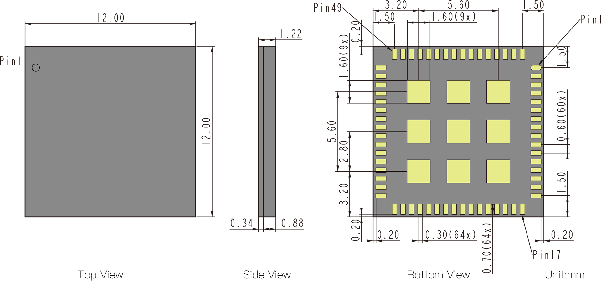 Figure 1: RAK3172-SiP mechanical dimension
Layout Recommendation
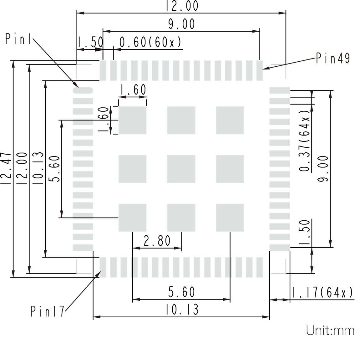 Figure 1: RAK3172-SiP layout
Environmental Characteristics
Operating Temperature
| Feature | Minimum | Typical | Maximum | Unit |
|---|---|---|---|---|
| Operating Temperature | -40 | 25 | 85 | °C |
Storage Temperature
| Feature | Minimum | Typical | Maximum | Unit |
|---|---|---|---|---|
| Storage Temperature | -40 | - | 85 | °C |
Recommended Reflow Profile
- On SMT reflow process, follow MSL3 (Moisture Sensitivity Level 3) guidance for PCBA assembly.
- Before SMT reflow, it is recommended to bake at 125° C for 12 hours first to reduce the risk of soldering issues and abnormalities.
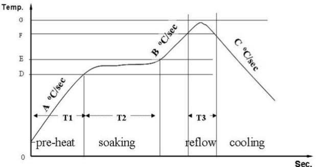 Figure 1: Reflow profile for RAK3172-SiP
Standard conditions for reflow soldering:
- Pre-heating Ramp (A) (Initial temperature: 150° C): 1~2.5° C/sec
- Soaking Time (T2) (110
190° C): **90120 sec** - Peak Temperature (G): 240~245° C
- Reflow Time (T3) (240-245° C): 50~70 sec
- Ramp-up Rate (B): 1-3° C/sec
- Ramp-down Rate (C): 1~5° C/sec
Software
Download the latest RAK3172-SiP WisDuo LPWAN SiP firmware provided below.
- The bin file contains the application code only and you need the RAK DFU Tool to upload this file to RAK3172-SiP via UART.
- The hex file contains both the bootloader and the application code. You need to use STM32CubeProgrammer to upload this.
RAK3172-SiP uses UART2 serial pins to upload the latest firmware.
Firmware/OS
Download the latest RAK3172-SiP and RAK3172LP-SiP firmware provided below.
| Model | Version | Source |
|---|---|---|
| RAK3172-SiP (.bin) | RUI3 (App only) | Download |
| RAK3172-SiP (.hex) | RUI3 (Bootloader and App) | Download |
| RAK3172LP-SiP (.bin) | RUI3 (App only) | Download |
| RAK3172LP-SiP (.hex) | RUI3 (Bootloader and App) | Download |
Models and Bundles
Ordering Information
| P/N | Model | Frequency | SKU |
|---|---|---|---|
| RAK3172-SIP-8-SM-NI | RAK3172-SiP | 8XX MHz for RU864/IN865/EU868 | 305041 |
| RAK3172-SIP-9-SM-NI | RAK3172-SiP | 9XX MHz for US915/AU915/KR920/AS923 | 306039 |
Certification

ANATEL Certification

CE Certification

FCC Certification

ISED Certification

JRL Certification

KC Certification

LoRaWAN Certification

RCM Certification

REACH Certification

RoHS Certification

RSM Certification

UKCA Certification

WPC Certification
For CE and FCC certifications we provide an AT command guide.
You can find it in our RUI3 documentation or get it from our Download Center.