RAK4600 Evaluation Board Datasheet
Overview
Description
RAK4600 Evaluation Board is designed to give you a quick start to explore the LoRa/LPWAN world. The board measures 30 x 60 mm and supports USB power supply, 3.7 V LiPo battery, and 5 V solar charging.
The board itself has the RAK4600 as its core, which is a module that utilizes Nordic nRF52832 MCU and an SX1276 LoRa chip. The high level of integration allows for outstanding performance: Lora TX Power of up to 20 dBm.
The board complies with LoRaWAN 1.0.2 specification, and it also supports LoRa P2P Point-to-Point communication. The low power, long-range LoRa communication capabilities of the board make it suitable for a variety of applications in the IoT field such as home automation, sensor networks, building automation, and personal area networks applications, such as health/fitness sensors and monitors.
Features
- LoRa module for Smart City, Smart Agriculture, Smart Industry
- Frequency range: 863–870 MHz (EU) / 902–928 MHz (US), ISM, and SRD systems
- I/O ports: UART/I2C/GPIO (optional NFC interface)
- Based on RAK4600 module with a sleep current consumption of 13.3 μA (down to 11.2 μA @ 2.0 V)
- LoRa Boost mode with 20 dBm output power
- BLE 5.0 (Tx power -20 to +4 dBm in 4 dB steps)
Specifications
Overview
Figure 1 and Figure 2 show the front and back views of the RAK4600 Evaluation Board front view.
 Figure 1: RAK4600 Evaluation Board Front Vew
 Figure 1: RAK4600 Evaluation Board Back View
Hardware
The hardware specification is categorized into five parts. It covers the interfaces, pin definitions and their corresponding functions. Also, it includes the RF requirements, electrical and mechanical parameters of the RAK4600 Evaluation Board.
Interfaces
RAK4601 is the WisBlock Core CPU module used on the RAK4600 Evaluation Board. Figure 3 shows an overview of interfaces found on the RAK4600 Evaluation Board.
 Figure 1: RAK4600 Evaluation Board Interface Overview
SWD Programming Interface
When programming via the RAKDAP1 DAPLink tool, it is required to have all of the following four (4) pins connected to your DAPLink tool:
- 3V3
- SWDIO
- SWCLK
- GND
For the aforementioned reason, it is best you leave these exposed for programming purposes and not to remap them as GPIOs.
Use Figure 4 as a guide to connect RAKDAP1 on the RAK4600 Evaluation Board.
 Figure 1: RAK4600 RAKDAP1 connection
For flashing the firmware, refer to the Flash the Firmware Using DAPLink and RAKDAP1 section.
RF Interface
The RF pins of the RAK4600 Evaluation Board are connected to external antennas through a standard iPEX antenna connector.
Use Figure 5 and Figure 6 as a reference to identify the antennas.
 Figure 1: RAK4600 Evaluation Board BLE antenna
 Figure 1: RAK4600 Evaluation Board LoRa antenna
Before powering the RAK4600 Evaluation Board, install the LoRa and BLE antenna first. Not doing so might damage the board.
Use Figure 7 as a reference to connect the antennas.
 Figure 1: RAK4600 Evaluation Board antenna connection
USB Interface
The Micro-B USB connector is compliant with the USB 2.0 specification. The pin definition of the USB interface is shown below:
| Pin Number | Pin Name | Description |
|---|---|---|
| 1 | USB_VBUS | (+5 V) USB Bus Voltage |
| 2 | USB_DM | USB Bus D+ positive pin |
| 3 | USB_DP | USB Bus D- negative pin |
| 4 | NC | Not connected |
| 5 | GND | Ground |
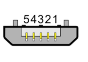 Figure 1: RAK4600 Micro-B USB connector
The USB data bus is connected to a USB-SERIAL CH340 chip. The CH340 is basically a USB bus convert chip that allows the USB to be converted to serial interface and serial interface pins converted to USB.
Pin Definition
The following tables below show the pin definitions of the RAK4600 Evaluation Board:
J10, J11, J12
On the RAK4600 Evaluation Board, there are three 2.54 mm pitch headers used for IO extension. Some data bus and signal from the MCU module are also connected to these headers, such as I2C, UART, ADC, etc.
J10 Pin Definition
| Pin Number | Pin Name | Description | Microcontroller Pin |
|---|---|---|---|
| 1 | BOOT0 | Boot for ST MCU | |
| 2 | VDD | Power supply generated by CPU module | |
| 3 | TX1/UART2_TX | UART2 TX pin | P0.19 |
| 4 | RX1/UART2_RX | UART2 RX pin | P0.18 |
UART serial pins on J10 are only useable as UART by developing custom FW that uses Nordic SDK. These pins can't be used as UART pins on the default RAK4600 FW or RUI compiled FW.
J11 Pin Definition
| Pin Number | Pin Name | Description | Microcontroller Pin |
|---|---|---|---|
| 1 | AIN0 | ADC input signal | |
| 2 | IO1 | General purpose IO | P0.14 |
| 3 | IO2 | Power switch control of 3V3_S | P0.17 |
| 4 | GND | Ground |
3V3_S is another 3.3 V power supply that can be controlled on/off by MCU. Set pin IO2=0 when the sensor is not in use to save power.
J12 Pin Definition
| Pin Number | Pin Name | Description | Microcontroller Pin |
|---|---|---|---|
| 1 | GND | Ground | |
| 2 | I2C1_SCL | I2C clock pin | P0.12 |
| 3 | I2C1_SDA | I2C data pin | P0.13 |
| 4 | VDD | Power supply generated by CPU module |
IO Module Connector Pin Definition
 Figure 1: RAK4600 IO Module Connector
| Pin Number | Pin Name | Description | Microcontroller Pin |
|---|---|---|---|
| 1 | VBAT | Li-Ion Battery positive pin | |
| 2 | VBAT | Li-Ion Battery positive pin | |
| 3 | GND | Ground | |
| 4 | GND | Ground | |
| 5 | 3V3 | 3.3 V power supply | |
| 6 | 3V3_S | 3.3 V power supply can be shutdown by CPU module | |
| 7 | USB+ | USB Bus D+ positive pin | Not connected |
| 8 | USB- | USB Bus D- negative pin | Not connected |
| 9 | VBUS | 5 V USB Bus Voltage | |
| 10 | SW1 | Switch signal for custom use | Not connected |
| 11 | TXD0 | UART1 TX pin | P0.23 |
| 12 | RXD0 | UART1 RX pin | P0.22 |
| 13 | RESET | Connected to the reset switch for MCU reset | P0.21 |
| 14 | LED1 | Red LED for battery charge indicator | |
| 15 | LED2 | Green LED for custom use | Not connected |
| 16 | LED3 | BLue LED for custom use | Not connected |
| 17 | VDD | Power supply generated by CPU module. Used to power sensor board if the MCU IO level is not 3.3 V | |
| 18 | VDD | Power supply generated by CPU module. Used to power sensor board if the MCU IO level is not 3.3 V | |
| 19 | I2C1_SDA | I2C data pin | P0.13 |
| 20 | I2C1_SCL | I2C clock pin | P0.12 |
| 21 | AIN0 | Analog Input for ADC | Not connected |
| 22 | AIN1 | Analog Input for ADC | Not connected |
| 23 | NC | Not connected | |
| 24 | NC | Not connected | |
| 25 | SPI_CS | SPI chip select signal | Not connected |
| 26 | SPI_CLK | SPI clock signal | Not connected |
| 27 | SPI_MISO | SPI MISO signal | Not connected |
| 28 | SPI_MOSI | SPI MISO signal | Not connected |
| 29 | IO1 | General Purpose IO | P0.14 |
| 30 | IO2 | Power switch control of 3V3_S | P0.17 |
| 31 | IO3 | General Purpose IO | P0.09 |
| 32 | IO4 | General Purpose IO | P0.10 |
| 33 | TX1/UART2_TX | UART2 TX pin | P0.19 |
| 34 | RX1/UART2_RX | UART2 RX pin | P0.18 |
| 35 | NC | Not connected | |
| 36 | NC | Not connected | |
| 37 | NC | Not connected | |
| 38 | NC | Not connected | |
| 39 | GND | Ground | |
| 40 | GND | Ground |
Sensor Module Connector Pin Definition
 Figure 1: Sensor Module Connector
Slot A
| Pin Number | Pin Name | Description | Microcontroller Pin |
|---|---|---|---|
| 1 | TX1/UART2_TX | UART2 TX pin | P0.19 |
| 2 | GND | Ground | |
| 3 | SPI_CS | SPI chip select signal | Not connected |
| 4 | SPI_CLK | SPI clock signal | Not connected |
| 5 | SPI_MISO | SPI MISO signal | Not connected |
| 6 | SPI_MOSI | SPI MOSI signal | Not connected |
| 7 | I2C1_SCL | I2C clock pin | P0.12 |
| 8 | I2C1_SDA | I2C data pin | P0.13 |
| 9 | VDD | Controlled by CPU module. Used to power sensor board if the MCU IO level is not 3.3 V | |
| 10 | IO2 | Power switch control of 3V3_S | P0.17 |
| 11 | 3V3_S | 3.3 V power supply can be shutdown by CPU module | |
| 12 | IO1 | General Purpose IO | P0.14 |
| 13 | NC | Not connected | |
| 14 | 3V3_S | 3.3 V power supply can be shutdown by CPU module | |
| 15 | NC | Not connected | |
| 16 | VDD | Controlled by CPU module. Used to power sensor board if the MCU IO level is not 3.3 V | |
| 17 | NC | Not connected | |
| 18 | NC | Not connected | |
| 19 | NC | Not connected | |
| 20 | NC | Not connected | |
| 21 | NC | Not connected | |
| 22 | NC | Not connected | |
| 23 | GND | Ground | |
| 24 | RX1/UART2_RX | UART2 RX pin | P0.18 |
Slot B
| Pin Number | Pin Name | Description | Microcontroller Pin |
|---|---|---|---|
| 1 | NC | Not connected | |
| 2 | GND | Ground | |
| 3 | SPI_CS | SPI Chip Select Pin | Not connected |
| 4 | SPI_CLK | SPI Clock signal | Not connected |
| 5 | SPI_MISO | SPI MISO signal | Not connected |
| 6 | SPI_MOSI | SPI MOSI signal | Not connected |
| 7 | I2C1_SCL | I2C clock pin | P0.12 |
| 8 | I2C1_SDA | I2C data pin | P0.13 |
| 9 | VDD | Controlled by CPU module. Used to power sensor board if the MCU IO level is not 3.3 V | |
| 10 | IO1 | General Purpose IO | P0.14 |
| 11 | 3V3_S | 3.3 V power supply can be shutdown by CPU module | |
| 12 | IO2 | Power switch control of 3V3_S | P0.17 |
| 13 | NC | Not connected | |
| 14 | 3V3_S | 3.3 V power supply can be shutdown by CPU module | |
| 15 | NC | Not connected | |
| 16 | VDD | Controlled by CPU module. Used to power sensor board if the MCU IO level is not 3.3 V | |
| 17 | NC | Not connected | |
| 18 | NC | Not connected | |
| 19 | NC | Not connected | |
| 20 | NC | Not connected | |
| 21 | NC | Not connected | |
| 22 | NC | Not connected | |
| 23 | GND | Ground | |
| 24 | NC | Not connected |
Slot C
| Pin Number | Pin Name | Description | Microcontroller Pin |
|---|---|---|---|
| 1 | NC | Not connected | |
| 2 | GND | Ground | |
| 3 | SPI_CS | SPI Chip Select Pin | Not connected |
| 4 | SPI_CLK | SPI Clock Pin | Not Connected |
| 5 | SPI_MISO | SPI MISO signal | Not connected |
| 6 | SPI_MOSI | SPI MOSI signal | Not connected |
| 7 | I2C1_SCL | I2C clock pin | P0.12 |
| 8 | I2C1_SDA | I2C data pin | P0.13 |
| 9 | VDD | Controlled by CPU module. Used to power sensor board if the MCU IO level is not 3.3 V | |
| 10 | IO4 | General Purpose IO | P0.10 |
| 11 | 3V3_S | 3.3 V power supply, can be shutdown by CPU module | |
| 12 | IO5 | General Purpose IO | Not connected |
| 13 | NC | Not connected | |
| 14 | 3V3_S | 3.3 V power supply, can be shutdown by CPU module | |
| 15 | NC | Not connected | |
| 16 | VDD | Controlled by CPU module. Used to power sensor board if the MCU IO level is not 3.3 V | |
| 17 | NC | Not connected | |
| 18 | NC | Not connected | |
| 19 | NC | Not connected | |
| 20 | NC | Not connected | |
| 21 | NC | Not connected | |
| 22 | NC | Not connected | |
| 23 | GND | Ground | |
| 24 | NC | Not connected |
Slot D
| Pin Number | Pin Name | Description | Microcontroller Pin |
|---|---|---|---|
| 1 | NC | Not connected | |
| 2 | GND | Ground | |
| 3 | SPI_CS | SPI Chip Select Pin | Not connected |
| 4 | SPI_CLK | SPI Clock Pin | Not connected |
| 5 | SPI_MISO | SPI MISO signal | Not connected |
| 6 | SPI_MOSI | SPI MOSI signal | Not connected |
| 7 | I2C1_SCL | I2C clock pin | P0.12 |
| 8 | I2C1_SDA | I2C data pin | P0.13 |
| 9 | VDD | Power supply generated by CPU module. Used to power sensor board if the MCU IO level is not 3.3 V | |
| 10 | IO6 | General Purpose IO | |
| 11 | 3V3_S | 3.3 V power supply, can be shutdown by CPU module | |
| 12 | IO5 | General Purpose IO | |
| 13 | NC | Not connected | |
| 14 | 3V3_S | 3.3 V power supply, can be shutdown by CPU module | |
| 15 | NC | Not connected | |
| 16 | VDD | Power supply generated by CPU module. Used to power sensor board if the MCU IO level is not 3.3 V | |
| 17 | NC | Not connected | |
| 18 | NC | Not connected | |
| 19 | NC | Not connected | |
| 20 | NC | Not connected | |
| 21 | NC | Not connected | |
| 22 | NC | Not connected | |
| 23 | GND | Ground | |
| 24 | NC | Not connected |
Battery Connector
The RAK5005 WisBase board can be powered by a battery via a P1 connector. The battery is not included in the RAK4600 Evaluation Board packaging.
Use Figure 11 as a reference to connect the battery.
 Figure 1: RAK4600 EVB battery and solar connector
The pin definition of the RAK600 Evaluation Board Li-Ion battery connector is shown in the table below. The matching connector for the battery wires is a JST PHR-2 2 mm pitch female.
P1 Battery Connector
| Pin | Pin Name | Description |
|---|---|---|
| 1 | GND | Ground |
| 2 | VBAT | Positive + pin of the battery |
The full specification of the RAK4600 Evaluation Board battery is shown in the table below.
| No. | Item | Specification |
|---|---|---|
| 1 | Charge Cut-off Voltage | 4.2 V |
| 2 | Nominal Voltage | 3.7 V |
| 3 | Discharge Cut-off Voltage | 2.75 V |
| 4 | Typical Capacity | 2650 mAh |
| 5 | Max Discharge Current | 0.5 C at 25 ℃ to 45 ℃ |
| 6 | PH Connector | 2.0 mm pitch |
| 7 | Cable Length | 110.0±3.0 mm |
| 8 | Cable Color | Red: VBAT, Black: GND |
- The voltage of the Li-Ion battery must not exceed 4.3 V.
- When connecting the battery, make sure the polarity is correct. Not all connectors are wired the same.
Solar Panel Connector
A 5 V solar panel can be connected to the board via the P2 connector to serve the purpose of charging the battery. The solar panel is not included on RAK4600 Evaluation Board packaging. Use Figure 11 as a guide to connect the solar panel.
The pin definition of the RAK4600 Evaluation Board solar panel connector is shown in the table below. The matching connector for the solar panel wires is an JST ZHR-2 1.5 mm pitch female.
P2 Solar Panel connector| Pin | Pin Name | Description |
|---|---|---|
| 1 | C0NN_5V | Positive + pin of solar panel |
| 2 | GND | GND |
The full specification of the Solar Panel for the RAK4600 Evaluation Board is shown in the table below.
| No. | Item | Specification |
|---|---|---|
| 1 | Nominal Voltage | 5 V |
| 2 | Typical Current | 80 mA |
| 3 | Size | Length: 60 mm, Width: 60 mm, Height: 2 mm |
| 4 | Connector | 1.5 mm pitch |
| 5 | Cable Color | Red: C0NN_5V, Black: GND |
The output of the solar panel must not exceed 5.5 V. Otherwise, it may cause permanent damage to the board.
LEDs
- 🔴 Red LED - connected to the charger chip to indicate the charger status. When the battery is charging, this red LED is on. When the battery is full, this LED is weak light or off.
RESET Button
The reset push button is connected to the reset pin P0.21 of the RAK4600. When pushed, it resets the MCU.
RF Switch Pin Definition
| LoRa Mode | VCTL1/P0.16 | VCTL2/P0.15 |
|---|---|---|
| Tx mode | H | L |
| Rx mode | L | H |
H: High Level 1.8 V to 5.0 V
L: Low Level 0 V
RF Characteristics
Operating Frequencies
The RAK4600 Evaluation Board supports the LoRaWAN high-frequency region, as shown in the table below.
| Module | Region | Frequency (MHz) |
|---|---|---|
| RAK4600(H) | Australia | AU915 |
| Asia | AS923 | |
| Europe | EU868 | |
| Canada | US915 | |
| India | IN865 | |
| Korea | KR920 | |
| North America | US915 |
Electrical Characteristics
Power Consumption
| Conditions | Current | Unit |
|---|---|---|
| Tx mode LoRa @17 dBm | 92 | mA |
| Tx mode LoRa @20 dBm | 125 | mA |
| Tx mode BT @4 dBm | 9 | mA |
| Rx mode LoRa @37.5 Kbps | 17 | mA |
| Rx mode BT @2 Mbps | 11.5 | mA |
Absolute Maximum Ratings
Exposure to maximum rating conditions may affect device reliability.
| Ratings | Maximum Value | Unit |
|---|---|---|
| VBUS power supply on USB port | -0.3 - 5.5 | V |
| VBAT battery voltage | -0.3 - 4.3 | V |
| C0NN_5V solar panel voltage | -0.3 - 5.5 | V |
| IO connector | -0.3 - VDD+0.3 | V |
| ESD | 2000 | V |
Mechanical Characteristics
Board Dimensions
Figure 10 shows the actual dimensions of the RAK4600 Evaluation Board measured in millimeters (mm).
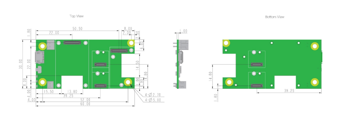 Figure 1: RAK4600 Evaluation Board dimensions
Certification

CE Certification

FCC Certification