Low Level Development Reference
Overview
RAK811 module comes with a standard version of firmware that allows you to configure its functionality via AT commands. This simplicity helps you develop LoRa(P2P) and LoRaWAN projects quickly.
Further customization of the firmware can be done through the RUI (RAKwireless Unified Interface) Online compiler. RAK's LoRaWAN node modules support not only out-of-the-box integration via AT commands but also allow you to customize RAK811 firmware and access other functionalities of the internal MCU using RUI API. More so, you can adapt and extend the logic in the firmware to meet your requirements.
Additionally, RAK offers a third alternative for advanced customers who need to have deeper integration of their solutions with these modules. In this alternative, you could develop your own version of STM32 firmware that runs inside of the RAK811 module.
How to Implement Your Own Firmware on RAK811 Module
Schematic
One of the essential aspects that allow customers to develop their own version of firmware is the RAK811 Hardware Schematic. This allows the customers to understand the module’s pinout and the connections between the internal STM32 MCU and the LoRa transceiver. Other important details can be found on RAK811 Datasheet.
There are two versions of the RAK811 module: the high-frequency bands RAK811(H) used on EU868, US915, AU915, KR920, AS923, and IN865, and the low-frequency bands RAK811(L) used on EU433 and CN470. These two modules have few differences in their schematic diagram that you should be aware of when you develop your own firmware.
Porting Lora Protocol Stack
When implementing the LoRa protocol stack, special attention must be given to the SPI connections since the LoRa transceivers are controlled by the MCU through an SPI interface. Hence, the following are the important pins: SPI1_MISO, SPI1_MOSI, SPI_NSS, SPI_CLK.
Additionally, the DIO pins and RF signal paths are significant as well to have functional LoRa communication. Another important thing to consider is the RF switch logic table. The complete details of pin connections can be found on the RAK811 Datasheet.
After that, the Real-Time Clock (RTC) must be properly configured in the MCU to ensure accurate timing of the protocol stack during the runtime. Finally, the protocol stack code can be added after configuring the other pins.
Application
Once the porting of the protocol stack is ready, you can focus on the development of their applications. There are two options you can choose with:
a. Develop your own bootloader.
b. Use RAK bootloader and the upgrade the custom firmware by using RAK Device Firmware Upgrade (DFU) Tool.
If you want to fully develop your own, you can refer to the schematic diagram and the datasheet of the MCU to implement the code. But if you want to use the RAK bootloader, continue reading the next section.
Bootloader
After the power is connected, the system bootloader will set up the Interrupt Vector table, initialize variables, and jump to the address of the main() symbol.
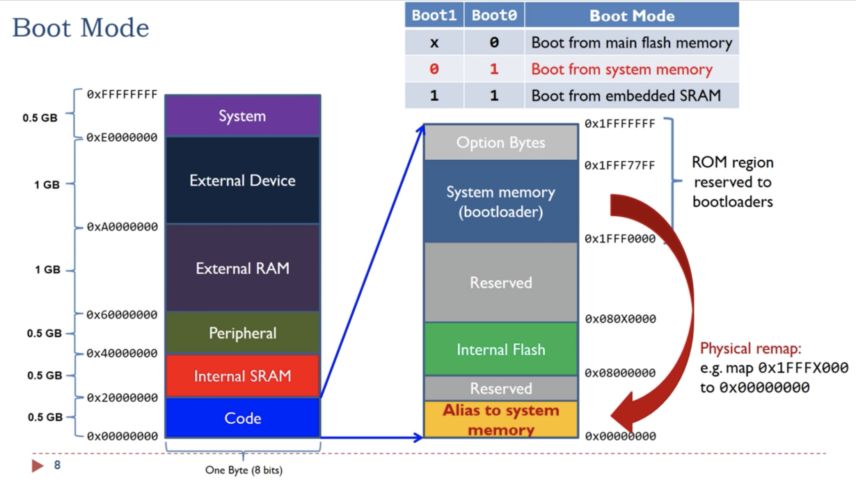
Figure 1 below shows the usual memory map of an ARM Cortex M3 MCU, which is the architecture of the MCU of the RAK811.
 Figure 1: Usual memory map for an ARM Cortex M3 MCU
The flash section is between the 0x0800 0000 and 0x080X 0000. X depends on the different models of MCU.
The RAK bootloader is stored in the internal flash section and has a size of 12K, located between 0x0800 0000 to 0x0800 2FFF. Its primary function is to write a new version of firmware received from the serial port into the flash memory section. The bootloader uses the Ymodem protocol and supervises all possible exceptions internally during the upgrade process. When the upgrade process is interrupted, the bootloader will detect abnormal events, and the FW upgrade will fail. You can perform the FW upgrade again using the bootloader after recycling the power.
The RAK811 bootloader uses flash memory segments between 0x0808 0F00 and 0x0808 0FFF to store its parameters. In the bootloader parameter storage area, 256 bytes are reserved for bootloading process, but only two words are used to store the jump flag and upgrade the status flag.
Finally, the serial port to communicate with the RAK bootloader in these modules is the UART1 (pin PA9, pin PA10). The parameters of the UART communication are the 115200 / 8-N-1, which need to be configured properly in the RAK firmware upgrade tool.
Application Requirements
Since the RAK bootloader is stored between the 0x0800 0000 and 0x0800 2FFF segments of the flash memory, your application should be shifted accordingly. In the application code, you need to modify the interrupt vector table address as the following:
SCB->VTOR = FLASH_BASE | 0x3000;
In the linker, the script must be updated accordingly. For example, in case you use GCC, modify your linker script like the following:
FLASH (rx): ORIGIN = 0x8003000, LENGTH = 116K
Your application firmware should implement as a minimum one AT command: at+boot\r\n. The function of this command is to jump from the application state into the bootloader state in preparation for the further application firmware upgrade. The logic of this command are the following:
-
For RAK811, write the value 0x00000000 into the address 0x0808 0F00.
-
Reset MCU. You can call the NVIC_SystemReset() interface in the ST library to reset the MCU.
The bootloader turned off the global interrupt when jumping from the application state. Therefore, when the application code is initialized, the global interrupt should be turned on again.
