RAK2011 WisLink Cellular BG96 Arduino Shield Datasheet
Overview
Description
The RAK2011 WisLink Cellular BG96 Arduino Shield is a compact cellular communications module that supports Low-Power Wide-Area (LPWA) technology for networking Internet-of-Things (IoT) devices. It can simultaneously support 2G, 4G/LTE, NB-IoT, and GPS, with an additional feature of Voice-over-LTE (VoLTE) for high definition (HD) and uninterrupted voice calls.
This multitude of features allows users the flexibility of migrating from 2G to 4G/LTE. It requires no hardware change and improves power consumption, system capacity, and spectrum efficiency by utilizing the Narrow Band Internet-of-Things, tracking units through GPS and location-based services (LBS), staying on the 4G/LTE network even when making or receiving calls, and other networking features.
The RAK2011 is based on the Quectel BG96 module and comes with drivers for Windows, Linux, and Android support via AT commands. It supports networking protocols such as PPP, TCP, UDP, SSL, TLS, FTP(S), HTTP(S), NITZ, PING, and MQTT. This is useful for facilitating software development and system integration into any IoT application.
RAK2011 can be used as a development platform in tandem with external microcontrollers/microprocessors-based platforms for IoT applications, or it can be used as a standalone device. It is in full compliance with FCC, CE, RoHS, and Japan TELEC/JATE.
Features
- Supports Low-Power Wide-Area (LPWA) Technology
- Features Voice-over-LTE (VoLTE) for high definition (HD) and uninterrupted voice calls
- Based on the Quectel BG96 module
- Supports networking protocols
- Flexible in migrating from 2G to 4G/LTE
Package Content
- BC96 LPWA IoT Cellular Arduino Shield
- Cellular Antenna
- GPS Antenna
Specifications
Overview
Board Overview
Figure 1 shows part identification on the top view of RAK2011 WisLink Cellular BG96 Arduino Shield.
 Figure 1: RAK2011 WisLink Cellular BG96 Arduino Shield Top View
The underside and dimension of the RAK2011 are shown in Figure 2.
 Figure 1: RAK2011 WisLink Cellular BG96 Arduino Shield Bottom View
Functional Diagram
The block diagram in Figure 3 shows the internal architecture and external interfaces.
 Figure 1: RAK2011 Functional Diagram
Hardware
The hardware specification is categorized into seven (7) parts. It discusses the interfacing of the module and its corresponding functions and diagrams. It also covers the electrical, environmental, mechanical, and antenna parameters that include the tabular data of the functionalities and standard values of the RAK2011 WisLink Cellular BG96 Arduino Shield.
Interfaces
The RAK2011 is built around the Quectel BG96 LPWA IoT cellular module and provides the following interfaces, headers, jumpers, buttons, and connectors:
- Micro-B USB
- Micro SIM Card Slot
- Arduino Headers (UART1, UART3, RESET, PWRKEY, STATUS, AP_READY, DTR, RI, PSM_IDC, W_DISABLE, 5 V, 3.3 V)
- 2x4 PCM Voice Headers (I2C, I2S)
- 2x3 Digital/Analog I/O Headers (ADC0, ADC1, GPIO0, GPIO1)
- 1x4 Debug UART Header (UART2)
- 1x2 USB BOOT Jumper
It has two push buttons to allow the user to power on/off and reset the board:
- POWER_KEY – Power on/off the BG96 module
- RESET – Reset the BG96 module
It has two SMA antenna connectors:
- Cellular (LTE/GSM) Antenna (3GPP Bands) – UART1
- GPS Antenna (1575.42±1.023 MHz) – UART3
Operating Modes
The RAK2011 WisLink Cellular BG96 Arduino Shield can operate in the following modes:
1. Normal Operation
- Idle: Software is active. The BG96 module has registered to the network and is ready to send and receive data.
- Talk/Data: Network connection is ongoing; the power consumption is determined by the network settings and data transfer rate.
2. Extended Idle Mode DRX (e-I-DRX)
BG96 module may negotiate with the network, via non-access stratum signaling, the use of e-I-DRX for reducing power consumption while being available for mobile terminating data and/or network originated functions within a certain period depending on the DRX cycle value.
3. Airplane Mode
AT+CFUN command or W_DISABLE# pin can set the module into airplane mode. In this case, RF functions are disabled.
4. Minimum Functionality Mode
AT+CFUN command can set the BG96 module into a minimum functionality mode without removing the power supply. In this case, both RF function and (U)SIM card will be disabled.
5. Sleep Mode
In this mode, the current consumption of the BG96 module will be reduced to a lower level. During this mode, the BG96 module can still receive paging messages, SMS and TCP/UDP data from the network.
6. Power Saving Mode (PSM)
The BG96 module may enter into Power Saving Mode for reducing its power consumption. PSM is similar to power-off, except the BG96 module remains registered on the network and there is no need to reestablish PDN connections.
7. Power OFF Mode
In this mode, the power management unit shuts down the power supply. The software is not active and the serial interfaces are not accessible, but the operating voltage remains applied.
Micro-B USB Interface
A standard Micro-B USB compliant with the USB 2.0 standard specification is used to provide an interface to connect to a PC for control of BG96 cellular modem and firmware upgrade.
 Figure 1: Micro-USB Interface
The Micro-B USB pin definition is shown below:
| Pin | Description |
|---|---|
| 1 | USB_VBUS (+5 V) |
| 2 | USB_DM |
| 3 | USB_DP |
| 4 | N/C |
| 5 | GND |
USB Boot Jumper
A standard two (2) pin USB Boot header (when closed) is used to force the RAK2011 to boot from USB port for performing a firmware upgrade.
 Figure 1: USB Boot Jumper
PWRKEY Push Button
PWRKEY push button is used to turn on/off the BG96 module. To turn on the BG96 module, push the PWRKEY button for at least 100 ms. The STATUS pin from Arduino header will output HIGH. To turn off the BG96 module, push PWRKEY button for at least 650 ms. STATUS pin from Arduino header will output LOW.
RESET Push Button
The RESET push button is used to reset the BG96 module. To reset the BG96 module, push the RESET button between 150 ms and 460 ms.
 Figure 1: PWRKEY and RESET Push Button
LED Indicators
Three LEDs are used to indicate the operating status. Below are the functions of the LEDs:
🔴 Red LED
- POWER ON: Indicates power status.
🟢 Green LED
- STATUS: Indicates module operation status.
🔵 Blue LED
- NETLIGHT: Indicates network activity status.
Pin Definition
Arduino Header
The mapping of Arduino headers on the RAK2011 WisLink Cellular BG96 Arduino Shield is shown in Figure 7.
 Figure 1: Pin Configurations for the Arduino headers
| Name | Pin | I/O | Description |
|---|---|---|---|
| UART1_TXD | D0 | D0 | UART1_TXD |
| UART1_RXD | D1 | D1 | Receive cellular (LTE/GSM) data |
| R1 | D2 | D0 | Ring indicator |
| DTR | D3 | D1 | Data Terminal Ready (sleep mode control) |
| AP_READY | D4 | D1 | Application processor sleep state detection |
| RESET | D5 | D1 | Reset signal of the BG96 module |
| PWRKEY | D6 | D1 | Turn on/off the BG96 module |
| STATUS | D7 | D0 | Indicate the BG96 module’s operation status |
| W_DISABLE | D8 | D1 | Airplane mode control |
| PSM_IND | D9 | D0 | Power saving mode indicator |
| UART3_RXD | D11 | D0 | Transmit GPS data |
| UART3_TXD | D12 | D1 | Receive GPS data |
-
UART1 interface supports 9600, 19200, 38400, 57600, 115200, 230400, 460800, and 921600 baud rates, and the default is 115200 bps. It is used for cellular (LTE/GSM) data transmission and AT command communication.
-
UART3 interface supports 115200 bps baud rate. It is used for outputting GPS data and NEMA sentences.
PCM Voice Header
A standard 2x4 (2.54 mm) male header is used to provide one Pulse Code Modulation (PCM) digital interface and one I2C interface to the external CODEC extension board.
 Figure 1: PCM Voice Header
PCM voice header pin definition is shown in the table below:
| Name | Pin | I/O | Description | Comments |
|---|---|---|---|---|
| I2C_SCL | 1 | OD | I2C serial clock | External pull-up resistor is required. 1.8 V only. Keep this open if unused. |
| I2C_SDA | 2 | OD | I2C serial data | |
| PCM_SYNC | 3 | DO | PCM frame sync output | 1.8 V power domain. Keep this open if unused. |
| PCM_CLK | 4 | DO | PCM clock output | |
| PCM_IN | 5 | DI | PCM data input | |
| PCM_OUT | 6 | DO | PCM data output |
The reference design for the external CODEC extension board is shown in Figure 9.
 Figure 1: External CODEC Extension Board
Analog Input & Digital I/O Header
A standard 2x3 (2.54 mm) male header is used to provide two (2) analog input (ADC0 and ADC1) and two (2) digital input and output port pins (GPIO0 and GPIO1) to an optional external extension board for additional features that may utilize these analog Input and digital I/O port pins. The analog input and digital I/O header pin layout are in Figure 10.
 Figure 1: Analog Input & Digital I/O Header
The analog Input/Digital I/O header signal definition is shown in the table below:
| Name | Pin | I/O | Description | DC Characteristics | Comments |
|---|---|---|---|---|---|
| GPIO0 | 1 | IO | General Purpose Input/Output | VOLmax=0.45 V VOHmin=1.35 V VILmin=0.3 V VILmax=0.6 V VIHmin=1.2 V VIHmax=2.0 V | 1.8 V power domain. Keep this open if unused. |
| GPIO1 | 2 | ||||
| ADC0 | 3 | AI | General Purpose Analog to Digital Converter | Voltage Range: 0.3 V to 1.8 V 15-bit resolution | Keep this open if unused. |
| ADC1 | 4 |
Debug Header
A standard 1x4 (2.54 mm) male header is used to provide a serial port (UART2) interface for debug and log output at 115200 bps baud rate. The debug header pin definition is shown in Figure 11.
 Figure 1: Debug Header
The analog Input/Digital I/O header signal definition is shown in the table below:
| Name | Pin | I/O | Description | DC Characteristics | Comments |
|---|---|---|---|---|---|
| DB_G_RXD | 2 | di | Receive Data | VILmin=0.3 V VILmax=0.6 V VIHmin=1.2 V VIHmax=2.0 V | 1.8 V power domain. Keep this open if unused. |
| DBG_TXD | 3 | DO | Transmit Data | VOLmmin=0 V VOLmax=0.45 V VOHmin=1.35 V VOHmax=1.83 V | 1.8 V power domain. Keep this open if unused. |
| ADC0 | 3 | AI | General Purpose Analog to Digital Converter | Voltage Range: 0.3 V to 1.8 V 15-bit resolution | Keep this open if unused. |
| ADC1 | 4 |
Antenna
 Figure 1: RAK2011 LTE and GNSS Antenna
Cellular (LTE/GSM)
Overview
The cellular (LTE/GSM) antenna for the RAK2011 covers the working frequency band from 824 MHz to 2690 MHz.
 Figure 1: Cellular Antenna
Antenna Dimension
 Figure 1: Cellular Antenna Dimension
Antenna Parameter
The Voltage Standard Wave Radio (VSWR) plot is shown in Figure 15.
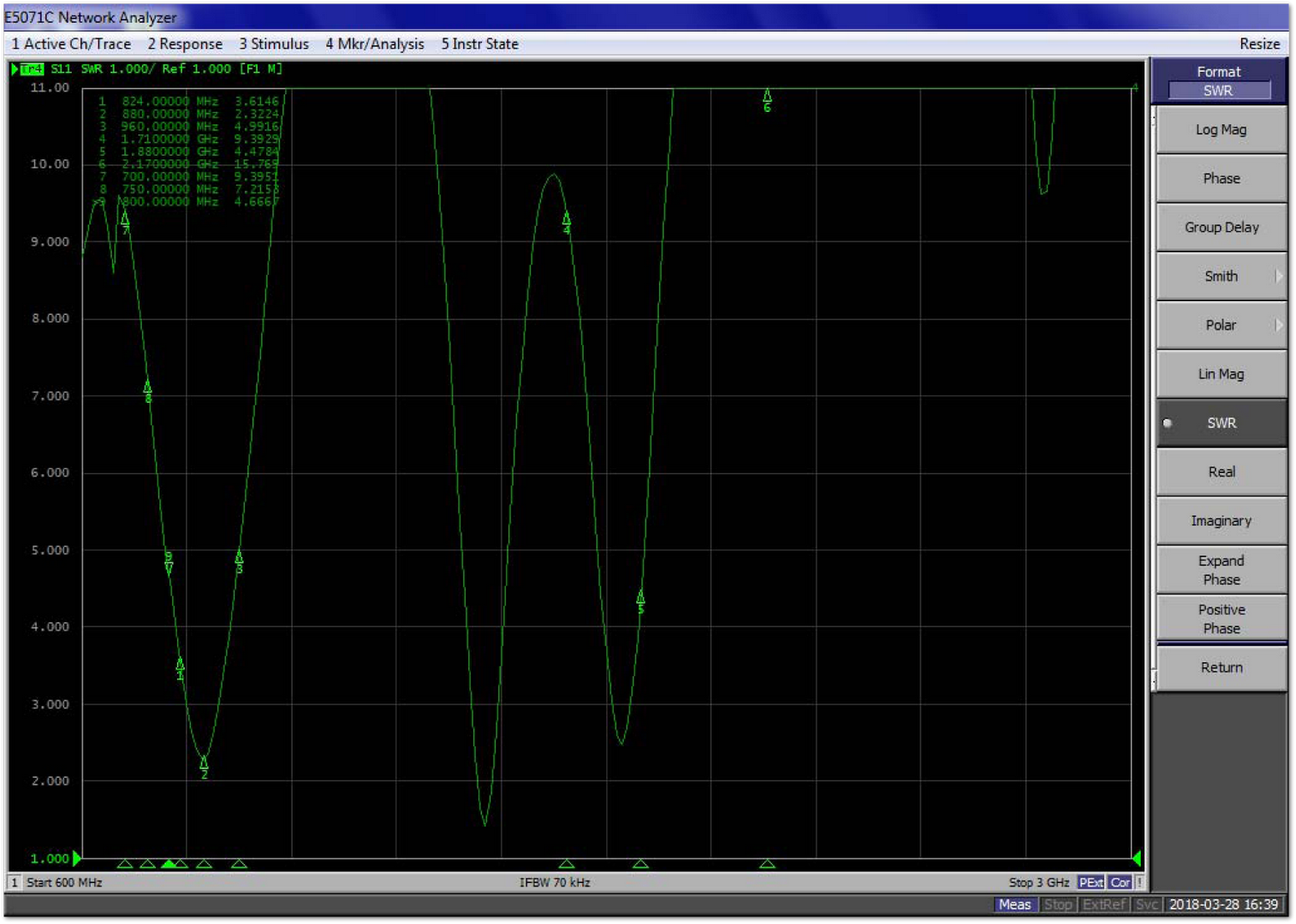 Figure 1: Cellular (LTE/GSM) Antenna Parameter
The VSWR data is shown in the table below:
| Frequency (MHz) | VSWR |
|---|---|
| 700 | 9.3 |
| 800 | 4.6 |
| 880 | 3.6 |
| 960 | 4.9 |
| 1710 | 9.3 |
| 1880 | 4.4 |
| 2170 | 15 |
The Smith plot is shown in Figure 16.
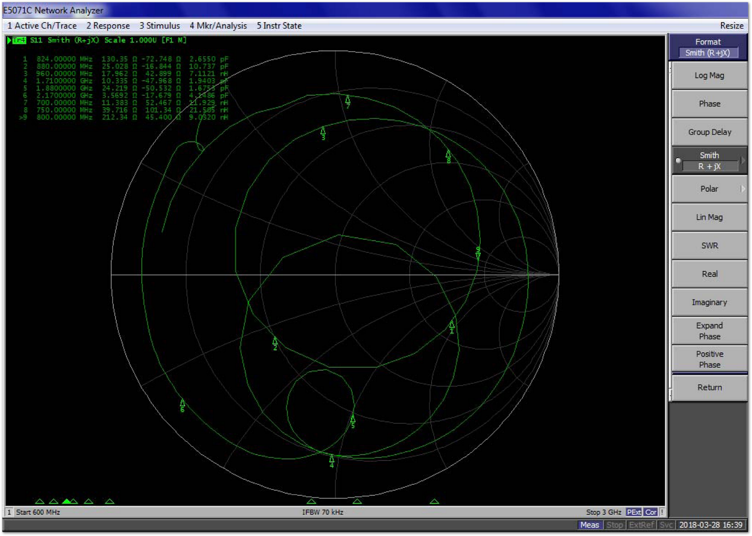 Figure 1: Smith Plot
Radiation Pattern on H-Plane
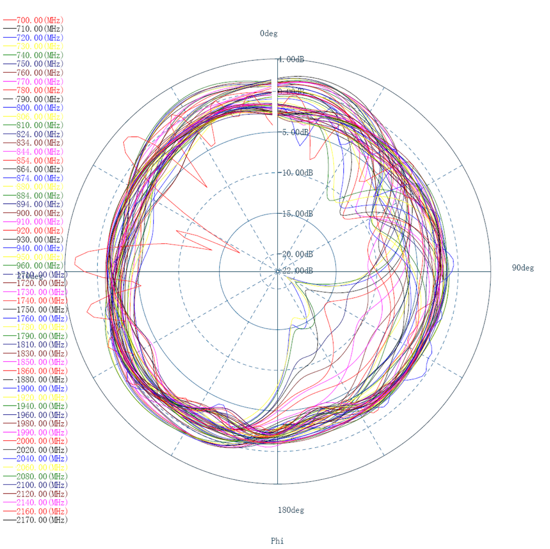 Figure 1: Radiation Pattern on H-Plane
Radiation Pattern on E1-Plane
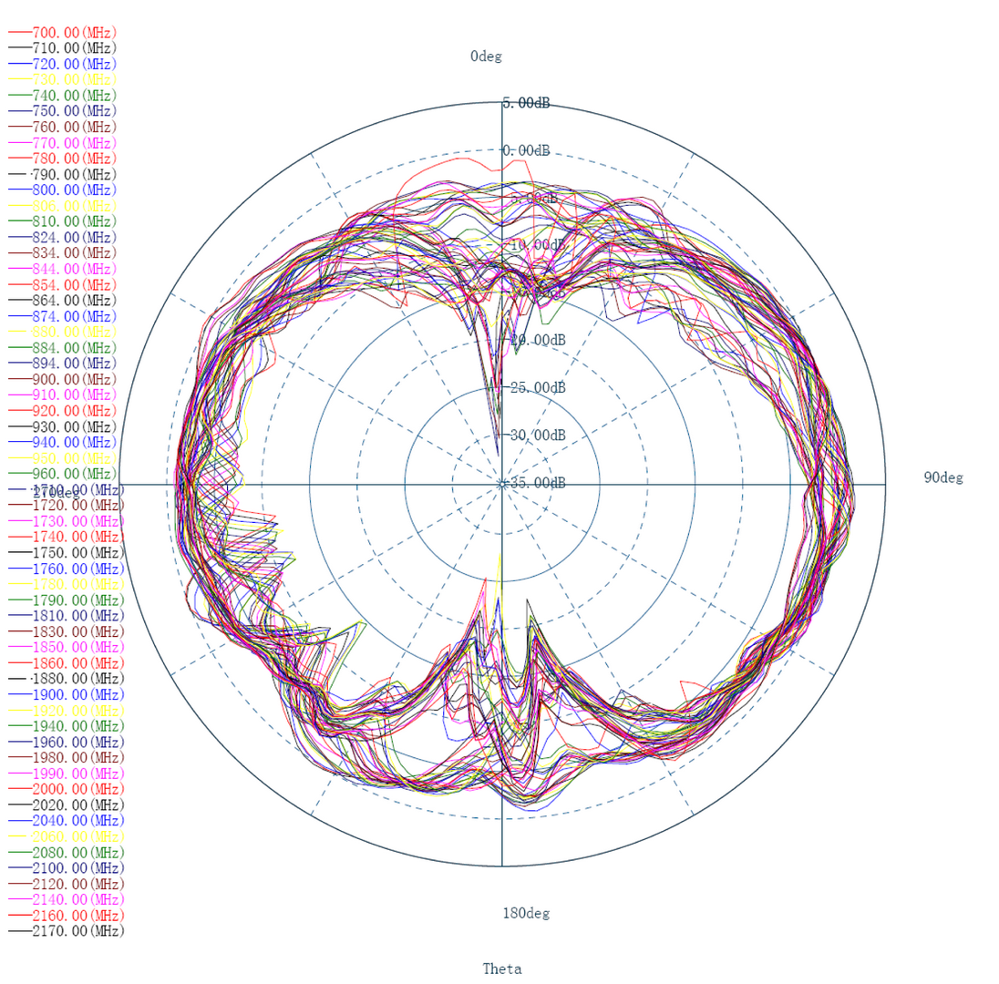 Figure 1: Radiation Pattern on E1-Plane
Radiation Pattern on E2-Plane
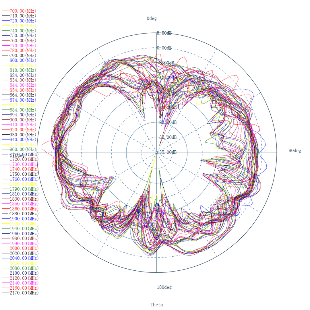 Figure 1: Radiation Pattern on E2-Plane
UGain and Efficiency Table
| Frequency (Hz) | Efficiency | Gain (dBi) | Frequency (Hz) | Efficiency | Gain (dBi) |
|---|---|---|---|---|---|
| 7.00E+08 | 49% | 1.632948 | 1.71E+09 | 35% | 0.02584 |
| 7.10E+08 | 51% | 1.826395 | 1.72E+09 | 35% | 0.0088 |
| 7.20E+08 | 49% | 1.833288 | 1.73E+09 | 36% | 0.647356 |
| 7.30E+08 | 44% | 1.600659 | 1.74E+09 | 44% | 0.806863 |
| 7.40E+08 | 46% | 1.896142 | 1.75E+09 | 35% | 0.03676 |
| 7.50E+08 | 50% | 1.936788 | 1.76E+09 | 46% | 0.549059 |
| 7.60E+08 | 50% | 1.721112 | 1.78E+09 | 34% | 0.14522 |
| 7.70E+08 | 46% | 1.406281 | 1.79E+09 | 35% | 0.41562 |
| 7.80E+08 | 45% | 1.491829 | 1.81E+09 | 36% | 0.35094 |
| 7.90E+08 | 47% | 1.8309 | 1.83E+09 | 34% | 0.30882 |
| 8.00E+08 | 45% | 1.843967 | 1.85E+09 | 38% | 0.430313 |
| 8.06E+08 | 41% | 1.714366 | 1.86E+09 | 35% | 0.33059 |
| 8.10E+08 | 45% | 2.215538 | 1.88E+09 | 37% | 0.008792 |
| 8.24E+08 | 42% | 1.97312 | 1.90E+09 | 43% | 0.479122 |
| 8.34E+08 | 44% | 1.890023 | 1.92E+09 | 40% | 0.111459 |
| 8.44E+08 | 42% | 1.407188 | 1.94E+09 | 46% | 0.407999 |
| 8.54E+08 | 42% | 1.453714 | 1.96E+09 | 44% | 0.037526 |
| 8.64E+08 | 47% | 2.111646 | 1.98E+09 | 48% | 0.405617 |
| 8.74E+08 | 46% | 1.93289 | 1.99E+09 | 48% | 0.112167 |
| 8.80E+08 | 48% | 1.960958 | 2.00E+09 | 47% | 0.144104 |
| 8.84E+08 | 46% | 1.930333 | 2.02E+09 | 46% | 0.14634 |
| 8.94E+08 | 52% | 2.347337 | 2.04E+09 | 47% | 0.033818 |
| 9.00E+08 | 50% | 2.192946 | 2.06E+09 | 45% | 0.112366 |
| 9.10E+08 | 50% | 2.265394 | 2.08E+09 | 51% | 0.672779 |
| 9.20E+08 | 49% | 2.081987 | 2.10E+09 | 48% | 0.291807 |
| 9.30E+08 | 48% | 2.005751 | 2.12E+09 | 54% | 0.939911 |
| 9.40E+08 | 49% | 2.128994 | 2.14E+09 | 54% | 1.161325 |
| 9.50E+08 | 49% | 2.305449 | 2.16E+09 | 59% | 1.631935 |
| 9.60E+08 | 48% | 2.233022 | 2.17E+09 | 59% | 1.967355 |
GPS Antenna
Overview
The GPS antenna for RAK2011 is shown in Figure 20.
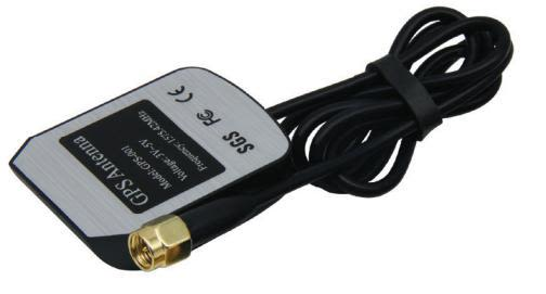 Figure 1: GPS Antenna
GPS Antenna Dimensions
 Figure 1: GPS Antenna Dimensions
GPS Environmental Requirements
The antenna environmental requirements are listed in the table below:
| Conditions | Temperature | Humidity |
|---|---|---|
| Working | -35 °C ~ +80 °C | 0% ~ 95% |
| Storage | -40 °C ~ +85 °C | 0% ~ 95% |
GPS Antenna Parameter
The GPS Antenna specifications and Post Environmental Tolerance (PET) are listed in the table below:
| Item | Specifications | PET |
|---|---|---|
| Range of Receiving Frequency | 1575.42±1.1 | ±2.5 |
| Center Frequency (MHz) w/ 30 mm2 GND plane | 1575.42 | ±3.0 |
| Bandwidth (MHz) (Return Loss ≤ -10 dB) | ≥10 | ±0.5 |
| VSWR (in Center Frequency) | ≤2.0 | ±0.5 |
| Gain (Zenith) (dBi Typ) w/ 70 mm2 GND Plane | 4.5 | ±0.5 |
| Axial Ratio (dB) w/ 70 mm2 GND Plane | 3.0 | ±0.2 |
| Polarization | Right-Handed Circular | - |
| Impedance (Ω) | 50 | - |
| Frequency/Temperature Coefficient (ppm/ºC) | 0±10 | - |
Amplifier Specifications are listed in the table below:
| Item | Specifications |
|---|---|
| Frequency Range | 1575.42 MHz |
| Gain | 27 dB |
| VSWR | ≤ 2.0 V |
| Noise Coefficient | ≤ 2.0 dBm |
| DC Voltage | 3 ~ 5 V |
| DC Current | 5 ± 2 mA |
Environmental test performance specifications are listed below:
| Item | Normal Temp. | High Temp. | Low Temp. |
|---|---|---|---|
| Amplifier Gain | 27 dB ± 2.0 | 27 dB ± 2.0 | 27 dB ± 2.0 |
| VSWR | ≤ 2.0 | ≤ 2.0 | ≤ 2.0 |
| Noise Coefficient | ≤ 2.0 | ≤ 2.0 | ≤ 2.0 |
-
High Temperature Test: Soak in temperature (85° C) and humidity (95%) chamber for 24-hour and return to normal temperature (at least for 1- hour) without visual shape change.
-
Low Temperature Test: Soak in temperature (-40° C) chamber for 24-hour and return to normal temperature (at least for 1-hour) without visual shape change.
RF Characteristics
Operating Frequency
The table below lists all the supported cellular (LTE/GSM) operating frequencies:
| 3GPP Band | Transmit (MHz) | Receive (MHz) |
|---|---|---|
| B1 | 1920 ~ 1980 | 2110 ~ 2170 |
| B2 (PCS1900) | 1850 ~ 1910 | 1930 ~ 1990 |
| B3 (DCS1800) | 1710 ~ 1785 | 1805 ~ 1880 |
| B4 | 1710 ~ 1755 | 2110 ~ 2155 |
| B5 (GSM850) | 824 ~ 849 | 869 ~ 894 |
| B8 (GSM900) | 880 ~ 915 | 925 ~ 960 |
| B12 | 699 ~ 716 | 728 ~ 746 |
| B13 | 777 ~ 787 | 746 ~ 757 |
| B18 | 815 ~ 829.9 | 860 ~ 874.9 |
| B19 | 830 ~ 844.9 | 875 ~ 889.9 |
| B20 | 832 ~ 862 | 791 ~ 821 |
| B26 | 814 ~ 848.9 | 859 ~ 893.9 |
| B28 | 703 ~ 748 | 758 ~ 803 |
| B39 | 1880 ~ 1920 | 1880 ~ 1920 |
Electrical Characteristics
Schematic Diagram
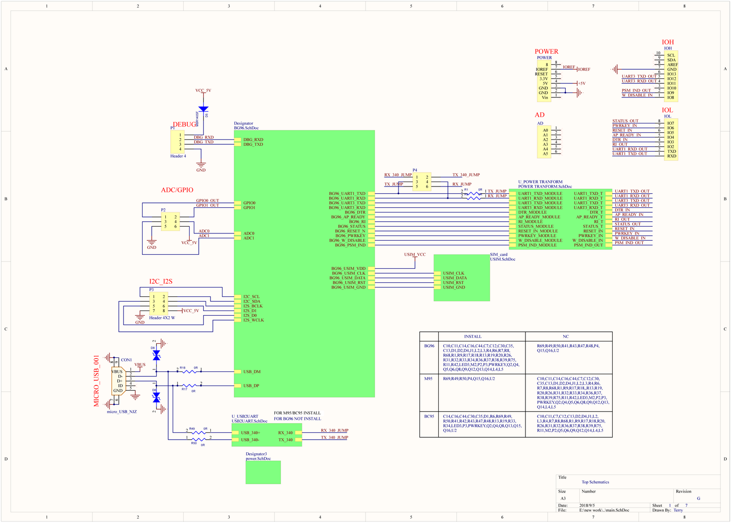 Figure 1: RAK2011 Schematic Diagram
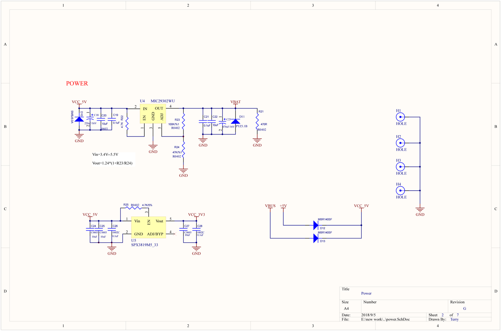 Figure 1: RAK2011 Power Schematic
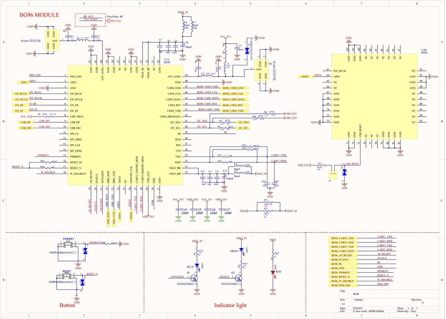 Figure 1: BG96 Module Schematic
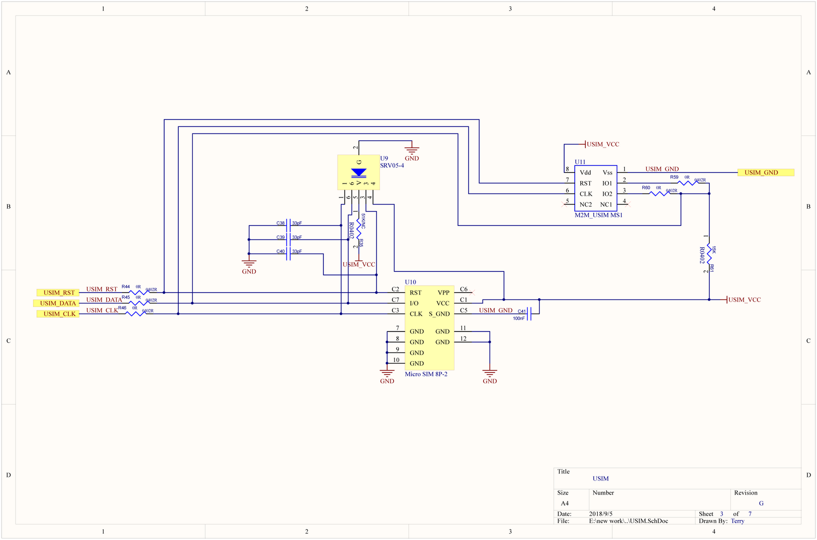 Figure 1: USIM Schematic
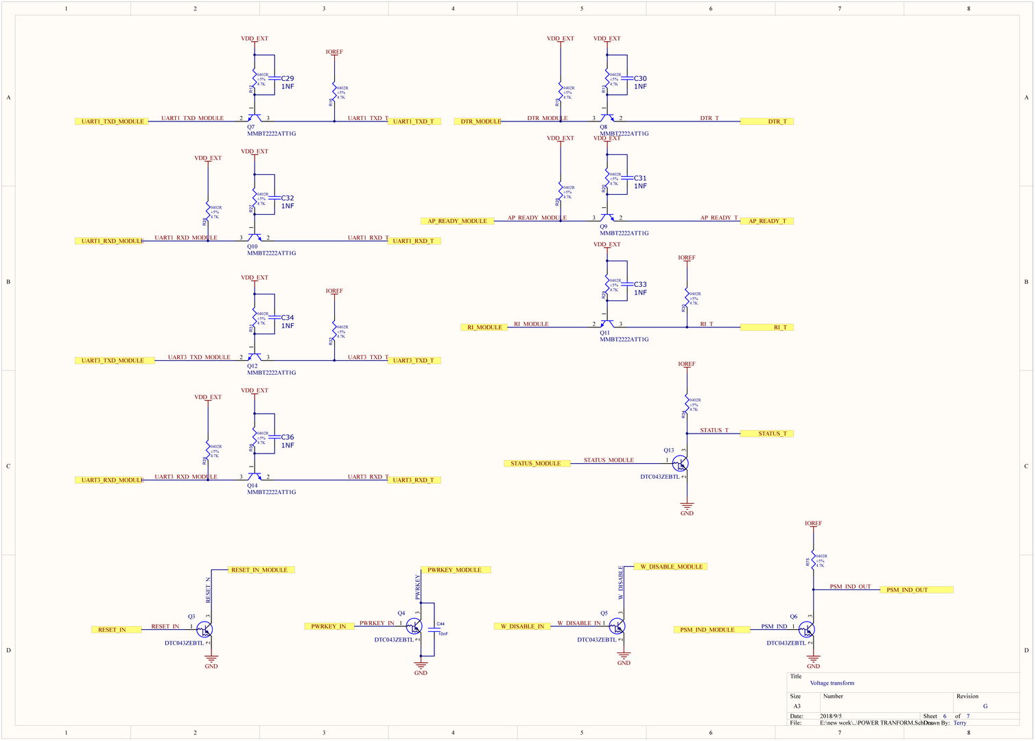 Figure 1: Voltage Transform
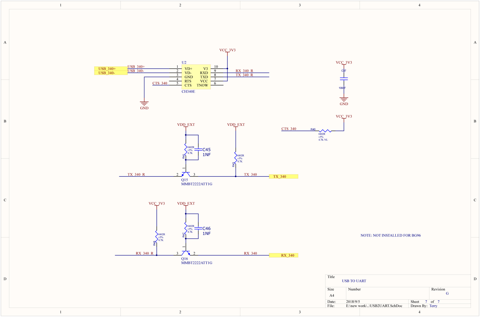 Figure 1: USB to UART Schematic
Power Requirements
The RAK2011 can be powered by +5 V from an MCU baseboard via Arduino header (POWER) if used as an Arduino Shield. It can also be powered by +5 V out of Micro-B USB if used as a standalone modem.
| Parameter | Min. | Max. |
|---|---|---|
| Power Supply Voltage | 3.7 V | 5.5 V |
| Current Consumption | - | 500 mA |
| Digital Input Voltage | 0 V | IOREF |
| Digital Output Voltage | 0 V | IOREF |
Environmental Characteristics
The table below lists the operation and storage temperature requirements:
| Parameter | Min. | Typical | Max. |
|---|---|---|---|
| Operation Temp. Range | -35° C | +25° C | +75° C |
| Extended Temp. Range | -40° C | - | +85° C |
| Storage Temp. Range | -40° C | - | +90° C |
