RAK5010-M WisTrio NB-IoT Tracker Datasheet
Overview
Description
The RAK5010-M-BG95 WisTrio NB-IoT Tracker is an advanced, highly flexible eMTC/NB-IoT/EGPRS tracker based on Quectel BG95-M3 (BG96 on the old model) LTE Cat M1&NB1, integrated with GPS, BLE, and a variety of sensors. The MCU running the board is a Nordic nRF52840 controller.
With the GPS and BLE features, the device can be used in a wide range of applications from outdoor to indoor scenarios where location-based services are necessary.
The board is equipped with two sensors on board: a humidity and temperature sensor and a 3-axis motion sensor. Additionally, the extension IOs in the module allow expandable sensor applications in addition to the onboard ones.
This board is particularly suitable to be used as a quick testing and prototyping tool for applications requiring Nb-IoT connectivity. Application development supports the GCC environment.
RAK5010-M-BG95 is an updated model of RAK5010-M. It uses the same circuit board and components except for the Quectel cellular modem used. The RAK5010-M-BG95 uses BG95-M3 while the original RAK5010-M-BG95 uses BG96. It shares the same AT commands set as well so if you are using the AT command interface, the two versions are compatible. If using a custom firmware (created with our RUI V2 or another IDE), you have to take into account that on the BG95-M3 you cannot use the cellular connection and the GNSS location acquisition at the same time. You have to stop the cellular connection before you can start the location acquisition.
Features
- Quectel BG95-M3 with LTE CAT M1, LTE NB1, EGPRS and GNSS
- Nordic nRF52840, with BLE 5.0 and long-range BLE
- nRF52840 integrates the ultra-low power microcontroller ARM Cortex-M4 (64 MHz)
- Built-in humidity and temperature sensor and 3-axis motion sensor
- iPEX connectors for the LoRa and GPS antenna and an on-board ceramic antenna for the BLE
- Nano SIM and ESIM options
- Can be powered by either Micro USB, 3.7 V rechargeable battery or a 5 V Solar Panel Port
- Multiple interfaces, I2C, UART, GPIO, and ADC
Specifications
Overview
The overview presents the RAK5010-M-BG95 WisTrio top view and its block diagram that shows the core of the board.
Module Overview
Figure 1 shows the top view and the interfaces of the RAK5010-M-BG95 NB-IoT tracker board.
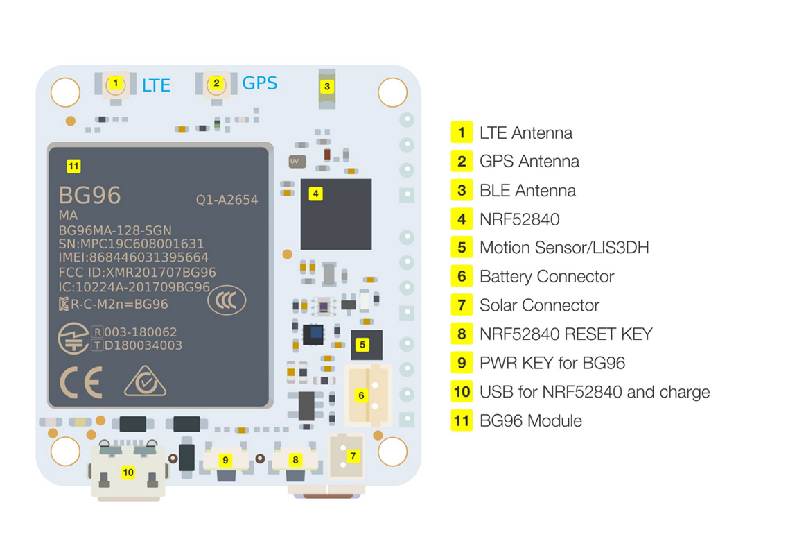 Figure 1: Top View of the Board with Interfaces
Figure 2 shows the bottom of the board. In Figure 3, the dimensions are shown, and Figure 4 shows the header pin spacing.
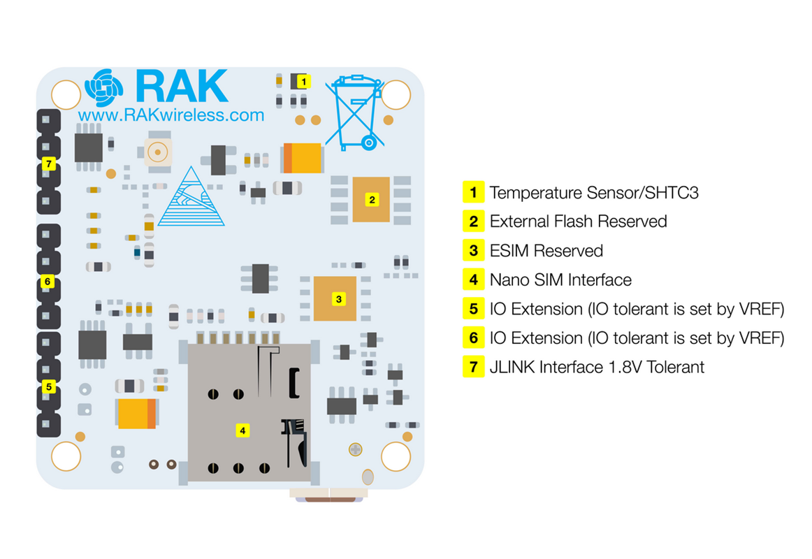 Figure 1: Bottom View of the Board with Interfaces
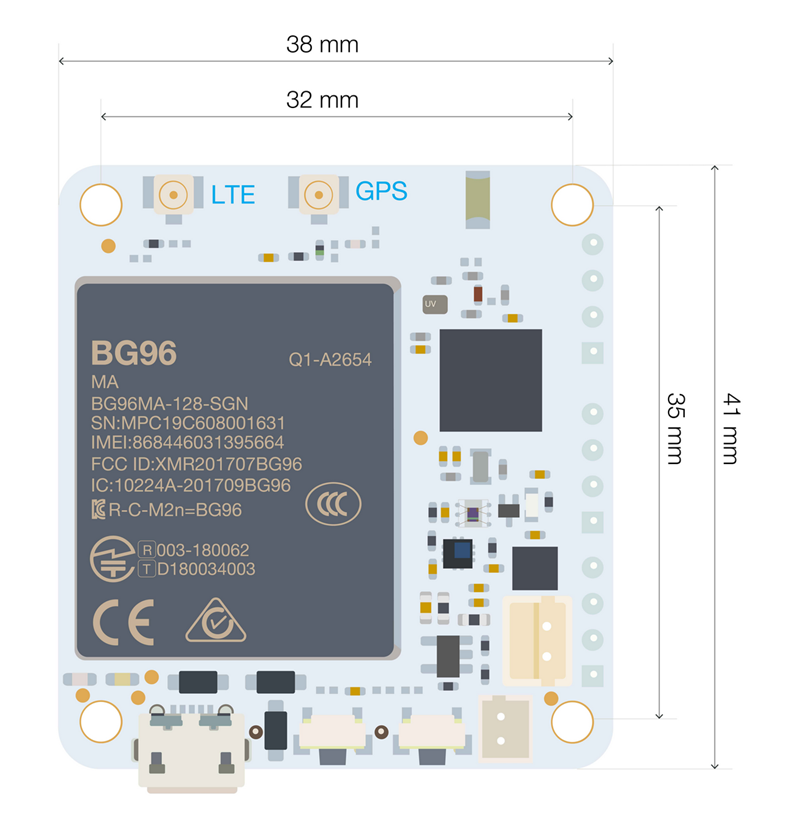 Figure 1: Board Dimensions
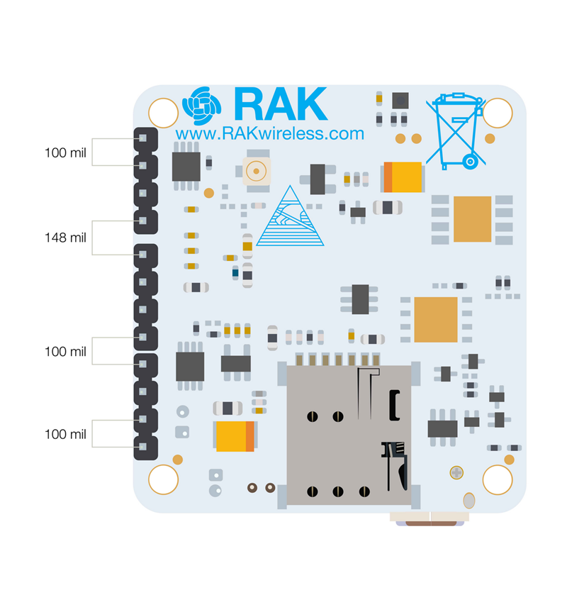 Figure 1: Header Spacing
Block Diagram
The block diagram below shows the internal architecture and external interfaces of the RAK5010-M-BG95 board.
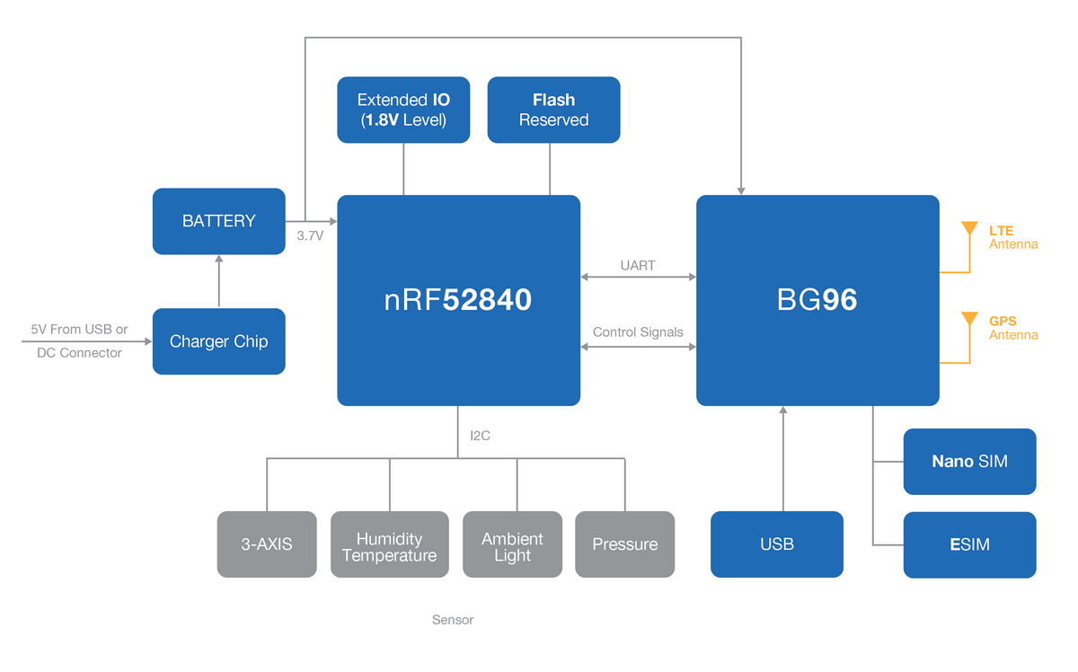 Figure 1: RAK5010-M-BG95 Block Diagram
Hardware
The hardware specification is categorized into seven parts. It discusses the interfacing, pinouts, and their corresponding functions and diagrams. It also covers the standard parameters of the board in terms of Electrical, Mechanical, and Environmental of which the tabular data of the functionalities and the standard values are presented. Moreover, a thorough discussion of the RAK5010-M-BG95 specification is included in this section.
Interfaces
The node is built around the BG95-M3 module and the nRF52840 BLE chip. It provides the following interfaces, headers, jumpers, buttons, and connectors:
- Micro USB
- 2 sets of 4-pin 2.54 mm Headers (UART, GPIOS, I2C, power)
- 4-pin J-LINK header
- 2-pin Battery female interface
- 2-pin Solar Panel female interface
- LEDs
- Reset Button
- PWR Button for the BG95-M3
There are two antenna connectors:
- LTE Antenna with iPEX connector
- GPS Antenna with iPEX connector
Micro-B USB Interface
A Standard Micro-B USB is compliant with USB 2.0 standard specification. This USB interface is connected to the USB port of NRF52840 by default. It also can connect to BG95-M3 by reworking some resistors on the board. If this USB port is connected to the BG95-M3, BG95-M3 AT command port, GNSS port, and debug port can be accessed through this USB. It is also used as a charge input port for the battery. The Micro-B USB pin definition is shown in Figure 6:
 Figure 1: USB Connector Pinout
| Pin | Description |
|---|---|
| 1 | USB_VBUS (+5 V) |
| 2 | USB_DM |
| 3 | USB_DP |
| 4 | NC |
| 5 | GND |
This USB port is also used as a port for charging the battery.
LEDs
Three LEDs are used to indicate operating status, here are their functions:
| Color | Connection | Function |
|---|---|---|
| 🟢 Green LED | connected to the nRF52840 | Defined by the user |
| 🔵 Blue LED | connect to the BG95-M3 | Indicates the status of the BG95-M3 |
| 🔴 Red LED | connect to the BG95-M3 | Indicates the network status of the BG95-M3 |
RESET Push Button
The Reset Push Button is used to reset the nRF52840. You can control the BG95-M3 reset with the firmware of the nRF52840.
PWRKEY Push Button
When the BG95-M3 is in power off mode, it can be turned back on to normal mode by holding the PWRKEY button for at least 100 ms. Holding the PWRKEY button for at least 650 ms, the module will execute the power-down procedure after the PWRKEY is released.
IO Connections between the BG95-M3 and the nRF52840
The nRF52840 communicates with the BG95-M3 primarily through the UART interface. There is, however, additional signaling between the two modules. This is for auto-monitoring of status indicators and control. The pin mapping is shown below:
| Function of BG95-M3 | PIN definition on nRF52840 |
|---|---|
| TX of UART | P0.08 (RX for the nRF52840) |
| RX of UART | P0.06 (TX for the nRF52840) |
| BG95-M3_CTS | P0.11 |
| BG95-M3_RTS | P0.07 |
| BG95-M3_RI | P0.27 |
| BG95-M3_STATUS | P0.31 |
| BG95-M3_RESET | P0.28 |
| BG95-M3_PWRKEY | P0.02 |
| BG95-M3_WDISABLE | P0.29 |
| BG95-M3_DTR | P0.26 |
| BG95-M3_AP READY | P0.30 |
| BG95-M3_PSM | P0.03 |
If BG95-M3_RESET, BG95-M3_PWRKEY, and BG95-M3_WDISABLE are not set correctly, the BG95-M3 module will not boot up normally. When powering up, the BG95-M3 RESET should be retained at a low-level voltage, the BG95-M3_WDISABLE should be retained at a low-level voltage, and the BG95-M3_PWRKEY should be given a pulse with a high level, and at least 100 ms width to turn the BG95-M3 normally.
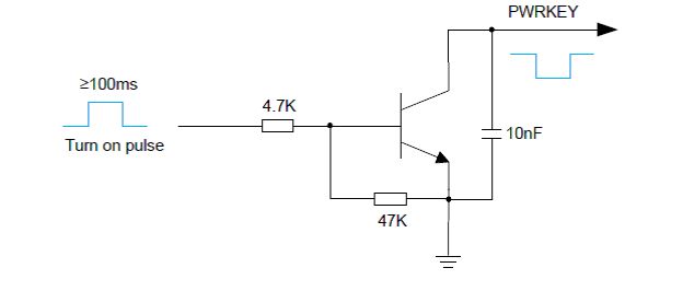 Figure 1: Turning on the BG95-M3 via the PWRKEY
Antenna Connector
The connectors for both the GPS and LTE antennas are iPEX. Make sure that the LTE antenna is tuned to work at the operational frequency of your LTE provider, corresponding to your region.
Pin Definition
There are two connectors on the board:
P1
Solar Panel Interface
| Pin | Pin Name | Description |
|---|---|---|
| 1 | C0NN_5V | Positive of Solar Panel |
| 2 | GND | GND |
The output of the solar panel cannot exceed 5.5 V. Otherwise, it may cause permanent damage to the board.
P2
Li-Ion Battery Connector
| Pin | Pin Name | Description |
|---|---|---|
| 1 | GND | GND |
| 2 | VBAT | Positive of the Battery |
J9
J9 is a J-LINK connector, with a J-LINK debugger, you can program and debug nRF52840.
| Pin | Pin Name | Description |
|---|---|---|
| 1 | VDD | 1.8 V default. Reference voltage for J-LINK, note 1 |
| 2 | SWDIO | SWD data signal(1.8 V tolerant) |
| 3 | SWDCLK | SWD clock signal(1.8 V tolerant) |
| 4 | GND | GND |
VDD of J9 should connect to the PIN1 of SEGGER J-LINK (see Figure 8) debugger for SWDIO/SWDCLK reference voltage. If this pin is not connected correctly, the J-LINK logic level may not match the required VDD for nRF52840, and it may damage the nRF52840.
Figure 8 shows the definition of a 20-Pin segger J-LINK connector:
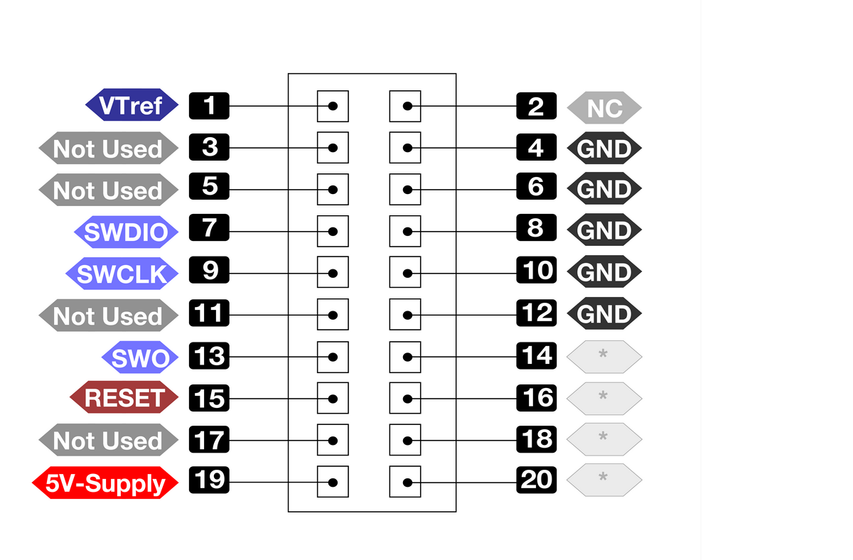 Figure 1: J-LINK Pinout
| Pin | Signal | Type | Description |
|---|---|---|---|
| 1 | VTref | Input | This is the target reference voltage. It is used to check if the target has power, to create the logic-level reference for the input comparators, and to control the output logic levels to the target. It is normally supplied from the VDD of the target board and must not have a series resistor. |
J10 and J12
J10 and J12 are IO extension headers. Those are bridged from the nRF52840 IOs, through logical level shift circuits. Thus, the IOs level is set by the VREF pin. The function of these IOs is configurable. They can work as UART, I2C, general GPIO, or ADC.
- Definition of J10:
| Pin | Pin Name | Description |
|---|---|---|
| 1 | GND | GND |
| 2 | VBAT | Connected to the Battery |
| 3 | AIN | Configurable IO, connected to AIN3 (P0.05) on nRF52840. If used as ADC, the input range is configurable. Refer to the manual of nrf52840. If used as general IO, the logic level is 1.8 V, and there is no level shift on it. |
| 4 | NRF_IO1 | Configurable IO, connected to P0.19 on the nRF52840. There is a level shift circuit between this pin and the nRF52840 |
- Definition of J12:
| Pin | Pin Name | Description |
|---|---|---|
| 1 | EXT_VREF | Reference level for the IO extensions |
| 2 | NRF_IO2 | Configurable IO, connect to P0.20 on the nRF52840. There is a level shift circuit between this pin and the nRF52840 |
| 3 | NRF_IO3 | Configurable IO, connect to P1.02 on the nRF52840. There is a level shift circuit between this pin and the nRF52840 |
| 4 | NRF_IO4 | Configurable IO, connect to P1.01 on the nRF52840. There is a level shift circuit between this pin and the nRF52840 |
The logic level shift circuit on the RAK5010-M-BG95 board connects EXT_VREF to your extension board’s power and equalizes it to the logical level of the IO on your extension board.
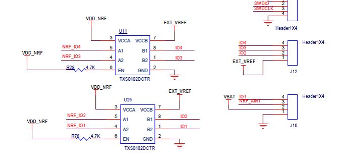 Figure 1: Typical Converter Circuitry
System on a Chip (SoCs) and Sensors
This section provides detailed specifications about the different modules present in the RAK5010-M-BG95 device.
1. BG95-M3 Module
BG95-M3 Frequency Bands
| LTE Bands | GSM | Rx-Diversity | GNSS |
|---|---|---|---|
| Cat M1 & NB1: | - | - | - |
| LTE-FDD: B1/B2/B3/B4/ B5/B8/B12/B13/B18/ B19/B20/B26/B28 | GSM850/GSM900 | Not Supported | GPS, GLONASS, BeiDou/ Compass, Galileo, QZSS |
BG95-M3 Key Features
| Feature | Details |
|---|---|
| Power Supply | Supply Voltage: 3.3 V – 4.3 V Typical supply voltage: 3.8 V |
| Transmitting Power | - Class: 3 (23 dBm ± 2 dB) for LTE-FDD bands - Class: 3 (23 dBm ± 2 dB) for LTE-TDD bands - Class: 4 (33 dBm ± 2 dB) for GSM850 Class: 4 (33 dBm ± 2 dB) for GSM900 - Class: 1 (30 dBm ± 2 dB) for DCS1800 Class: 1 (30 dBm ± 2 dB) for PCS1900 Class: E2 (27 dBm ± 3 dB) for GSM850 8-PSK Class: E2 (27 dBm ± 3 dB) for GSM900 8-PSK Class: E2 (26 dBm ± 3 dB) for DCS1800 8-PSK Class: E2 (26 dBm ± 3 dB) for PCS1900 8-PSK |
| LTE Features | - Supports LTE Cat M1 and LTE Cat NB1 - Supports 1.4 MHz RF bandwidth for LTE Cat M1 - Supports 200 kHz RF bandwidth for LTE Cat NB1 - Supports SISO in the DL direction Cat M1: Max. 300 Kbps (DL)/375 Kbps (UL) Cat NB1: Max. 32 Kbps (DL)/70 Kbps (UL) |
| GSM Features | GPRS: - Supports GPRS multi-slot class 33 (by default) - Coding scheme: CS-1, CS-2, CS-3, and CS-4 Max. 107 Kbps (DL), Max. 85.6 Kbps (UL) EDGE: - Supports Edge multi-slot class 33 (by default) - Supports GMSK and 8-PSK for different MCS Downlink - Coding Schemes: CS 1-4 and MCS 1-9 Uplink Coding Schemes: CS 1-4 and MCS 1-9 Max. 296 Kbps (DL), 236.8 Kbps (UL) |
2. nRF52840 Module
| Parameter | Detail |
|---|---|
| CPU | ARM® Cortex®-M4 32-bit processor with FPU, 64 MHz |
| Flash | 1 MB |
| RAM | 256 KB |
| BLE Protocol | BLE 5.0 |
| BLE Tx Power | 8 dBm max |
| BLE Rx Sensitivity | 95 dBm @ 1 Mbps BLE mode |
| BLE Data Rate | 2 Mbps, 1 Mbps, 500 Kbps, 125 Kbps |
| Current Consumption | 4.8 mA in Tx, 4.6 mA in Rx, and 1.5 uA in Sleep Mode |
3. Humidity and Temperature Sensors
The Temperature and Humidity Sensor is an SHTC3 from Sensirion.
Temperature
| Parameter | Conditions | Value | Units |
|---|---|---|---|
| Accuracy | Typ | ±2.0 | ° C |
| Tolerance | Max | See Figure 2 | ° C |
| Repeatability | - | 0.1 | ° C |
| Resolution | - | 0.01 | ° C |
| Specified Range | - | -40 to +125 | ° C |
| Response Time | τ 63% | < 5 to 30 | s |
| Long-term Drift | Typ. | < 0.2 | ° C/y |
Humidity
| Parameter | Conditions | Value | Units |
|---|---|---|---|
| Accuracy | Typ | ±2.0 | %RH |
| Tolerance | Max | See Figure 2 | %RH |
| Repeatability | - | 0.1 | %RH |
| Resolution | - | 0.01 | %RH |
| Hysteresis | - | ±1 | %RH |
| Specified Range | Extended | 0 to 100 | %RH |
| Response Time | τ 63% | 8 | s |
| Long-term Drift | Typ. | < 0.25 | %RH/y |
4. 3-Axis Motion Sensor
| Symbol | Parameter | Test Condition | Min. | Typ. | Max. | Unit |
|---|---|---|---|---|---|---|
| FS | Measurement Range | FS bit set to 00 | ±2.0 | g | ||
| FS bit set to 01 | ±4.0 | g | ||||
| FS bit set to 10 | ±8.0 | g | ||||
| FS bit set to 11 | ±16.0 | g | ||||
| So | Sensitivity | FS bit set to 00; High-resolution mode | 1 | mg/digit | ||
| FS bit set to 00; Normal mode | 4 | mg/digit | ||||
| FS bit set to 00; Low Power mode | 16 | mg/digit | ||||
| FS bit set to 01; High-resolution mode | 2 | mg/digit | ||||
| FS bit set to 01; Normal mode | 8 | mg/digit | ||||
| FS bit set to 01; Low-power mode | 32 | mg/digit | ||||
| FS bit set to 10; High-resolution mode | 4 | mg/digit | ||||
| FS bit set to 10; Normal mode | 16 | mg/digit | ||||
| FS bit set to 10; Low-power mode | 64 | mg/digit | ||||
| FS bit set to 11; High-resolution mode | 12 | mg/digit | ||||
| FS bit set to 11; Normal mode | 48 | mg/digit | ||||
| FS bit set to 11; Low-power mode | 192 | mg/digit |
Antennas
1. LTE Antenna
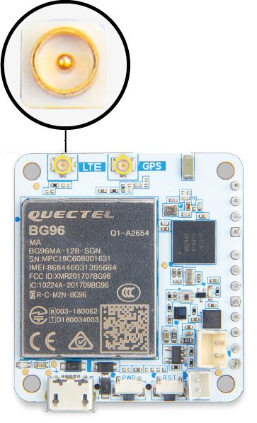 Figure 1: iPEX onboard connector for the LTE antenna
A PCB antenna (Figure 11) is included with the board. In case you want to use another antenna, keep in mind that you need to have the proper connector (iPEX) and have it tuned to the frequency band of operation in your region.
 Figure 1: PCB LTE Antenna with Pigtail
LTE Antenna Specifications
| Item | Specifications |
|---|---|
| Range of Frequency | 806-960/1710-2700 MHz |
| VSWR | ≤1.5 |
| Gain | 1.0 |
| Polarization | Linear |
| Impedance (Ω) | 50 |
| Antenna Type | PCB |
LTE Antenna Environmental Requirements
The antenna environmental requirements are listed in the table below:
| Conditions | Temperature | Humidity |
|---|---|---|
| Working | -40° C ~ +75° C | 0% ~ 95% |
| Storage | 40° C ~ +85° C | 0% ~ 95% |
2. GPS Antenna
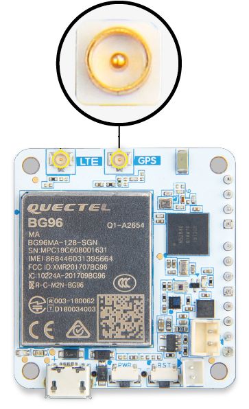 Figure 1: iPEX onboard connector for the GPS antenna
GPS Antenna Power Supply Control
To support low power and long battery life, the active GPS antenna power supply should be shut down when the system doesn’t access the data from the GPS module. The GPS power supply is controlled by nRF52840 with MOSFET. The pin map of GPS_EN on Nrf52840 is P1.07 and the circuit is shown in Figures 13 and 14:
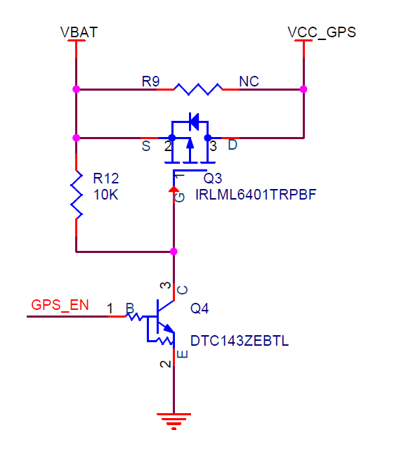 Figure 1:
  Figure 1: iPEX onboard connector for the GPS antenna
- Set P1.07=1, GPS antenna power is on.
- Set P1.07=0, GPS antenna power is off.
GPS Antenna Specifications
 Figure 1: GPS Antenna
| Item | Specifications | PET |
|---|---|---|
| Range of Receiving Frequency | 1575.42±1.1 | ±2.5 |
| Center Frequency (MHz) w/ 30 mm2 GND plane | 1575.42 | ±3.0 |
| Bandwidth (MHz) (Return Loss ≤ -10 dB) | ≥10 | ±0.5 |
| VSWR (in Center Frequency) | ≤1.5 | ±0.5 |
| Gain (Zenith) (dBi Typ.) w/ 70 mm2 GND Plane | 4.5 | ±0.5 |
| Axial Ratio (dB) w/ 70 mm2 GND Plane | 3.0 | ±0.2 |
| Polarization | Right-Handed Circular | - |
| Impedance (Ω) | 50 | - |
| Frequency Temperature Coefficient (ppm/ºC) | 0±10 | - |
GPS Antenna Amplifier Specifications
| Item | Specifications |
|---|---|
| Frequency Range | 1575.42 MHz |
| Gain | 27 dB |
| VSWR | ≤ 2.0 V |
| Noise Coefficient | ≤ 2.0 dB |
| DC Voltage | 3 ~ 5 V |
| DC Current | 10 mA |
GPS Antenna Environmental Test Performance Specifications
| Item | Normal Temp. | High Temp. | Low Temp. |
|---|---|---|---|
| Amplifier Gain | 27 dB ± 2.0 | 27 dB ± 2.0 | 27 dB ± 2.0 |
| VSWR | ≤ 2.0 | ≤ 2.0 | ≤ 2.0 |
| Noise Coefficient | ≤ 2.0 | ≤ 2.0 | ≤ 2.0 |
High-temperature test: Soap in temperature (85° C) and humidity (95%) chamber for 24 hours and return to normal temperature (at least for 1 hour) without visual shape change.
Low-temperature test: Soap in temperature (-40° C) chamber for 24 hours and return to normal temperature (at least for 1 hour) without visual shape change.
GPS Antenna Environmental Requirements
| Conditions | Temperature | Humidity |
|---|---|---|
| Working | -35° C ~ +80° C | 0% ~ 95% |
| Storage | -35° C ~ +80° C | 0% ~ 95% |
Electrical Characteristics
Schematic Diagram
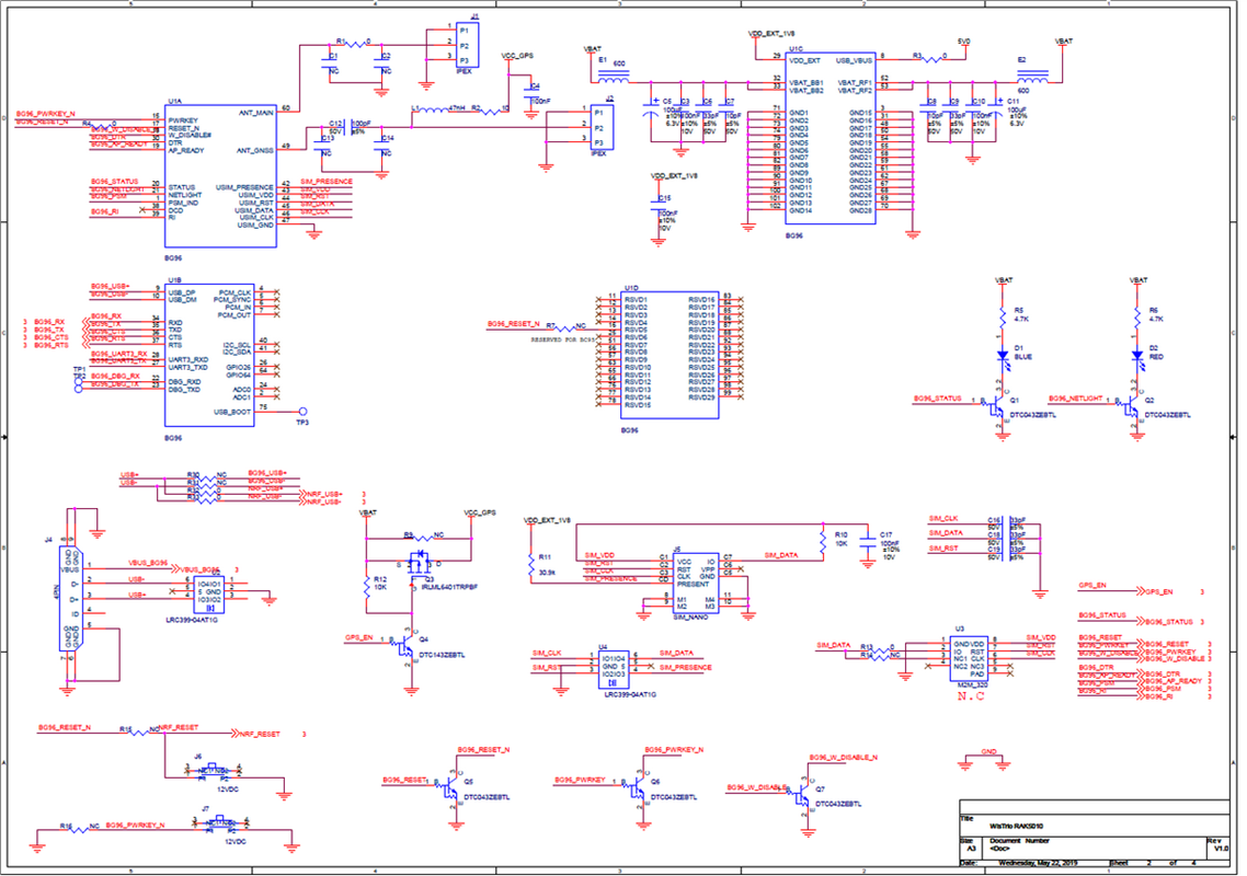 Figure 1: Schematic Diagram Part 1
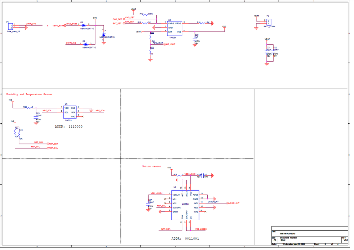 Figure 1: Schematic Diagram Part 2
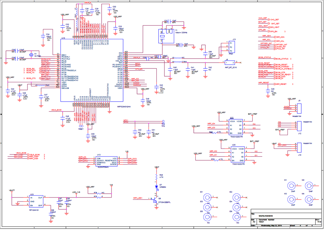 Figure 1: Schematic Diagram Part 3
Absolute Maximum Ratings
Functional operation of the device under the conditions listed is not advised. Hence, exposure to maximum rating conditions may affect device reliability.
| Ratings | Maximum Value (V) |
|---|---|
| Vbus, power supply on UBS port | -0.3 - 5.5 |
| Vbat, battery voltage | -0.3 - 4.3 |
| Vconn solar panel voltage | -0.3 - 5.5 |
| IOs of J-link (J9) | -0.3 - 1.9 |
| IOs of BG95-M3, nRF52840 - J10 and J12 | -0.3 -VREF |
| ESD | 2000 |
The RAK5010-M, like any electronic equipment, is sensitive to electrostatic discharge (ESD). Improper handling can cause permanent damage to the module.
Current Consumption
| Conditions | Current |
|---|---|
| The nRF52840 is Running, the BG95-M3 transmits data @ NB1, 23 dBm | 200 mA |
| BLE transmits @ 0 dBm, the BG95-M3 is in power saving mode | 7 mA |
| The nRF52840 is in sleep mode, the BG95-M3 is in power saving mode | 13 µA |
For the above results to be reached, the nRF52840 regulator has to be in DC-DC mode and all the sensors have to be in sleep mode.
Power Requirements
The RAK5010-M-BG95 tracker board can be powered by a battery, connected to the P2. The nominal operational voltage of the battery should be within the range in the table:
| Min | Type | Max | Unit |
|---|---|---|---|
| 3.3 | 3.7 | 4.3 | V |
If a rechargeable battery is used, the USB connector is used as a charging port. The voltage and current supplied to the battery through the port should not exceed the ones in the table below.
| Parameter | Value |
|---|---|
| Charging Voltage | 4.5-5.5 V |
| Charging Current | 500 mA |
A suitable Li-Ion battery would have the following parameters:
| Parameter | Value |
|---|---|
| Standard Voltage | 3.7 V |
| Charging Voltage | 4.2 V |
| Capacity | As required |
| Discharge Current | 2 A |
A 5 V solar panel can be connected to the board via the P1 connector to serve the purpose of charging the battery.
To avoid damage both to the battery and board:
- Do not power the USB port if a non-rechargeable battery is connected to the RAK5010-M.
- Do not attach the solar panel if the non-rechargeable battery is used.
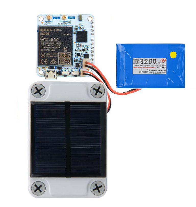 Figure 1: Battery Charging via Solar Panel
Laboratory Testings
Figure 20 and Figure 21 display the average current consumption based on the different test cases.
Equipments:
- Oscilloscope
- RAK5010-M-BG95 WisTrio NB-IoT Tracker Pro
Cellular Packet Sending
The RAK5010-M-BG95 WisTrio NB-IoT Tracker Pro takes 489.733 ms to send a Cellular packet which consumes 64.9 mA of current.
- Sending Time: 489.733 ms
- Current consumption: 64.9 mA
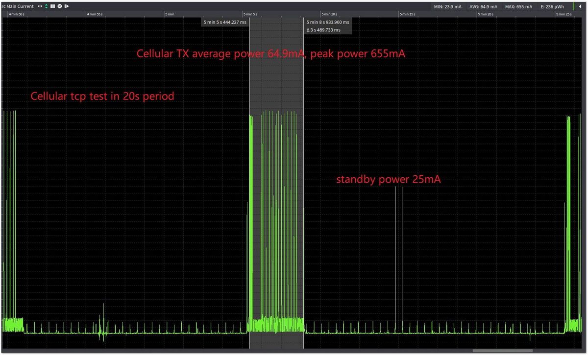 Figure 1: Oscilloscope Screen Capture of Cellular Packet Sending
Sleep Mode
The RAK5010-M-BG95 WisTrio NB-IoT Tracker Pro when in sleep mode consumes 20.5 uA of current.
- Current consumption: 20.5 uA
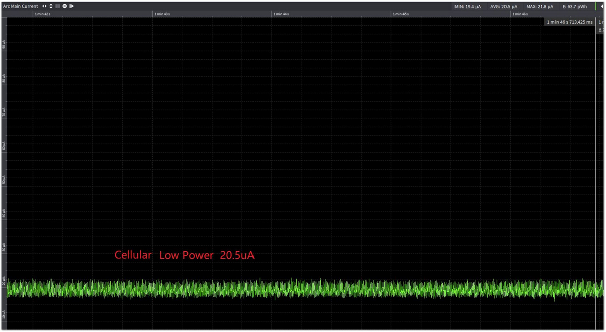 Figure 1: Oscilloscope Screen Capture of RAK5010-M-BG95 LoRa Module in Sleep Mode
Mechanical Characteristics
Module Dimensions
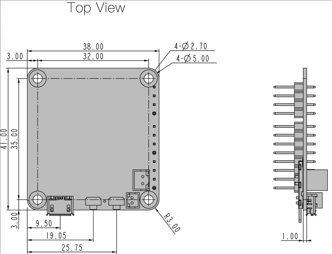 Figure 1: Top View
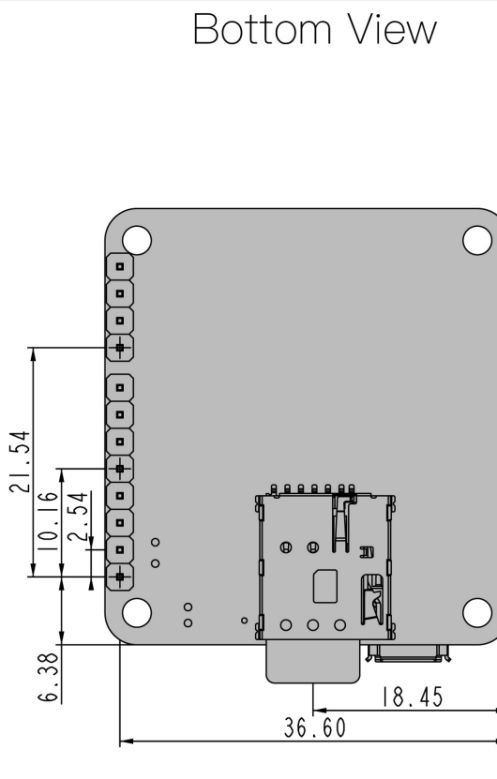 Figure 1: Bottom View
Environmental Characteristics
The table below lists the operation and storage temperature requirements:
| Parameter | Min | Typical | Max |
|---|---|---|---|
| Operational Temp. Range | -35° C | +25° C | +75° C |
| Extended Temp. Range | -40° C | +25° C | +80° C |
| Storage Temp. Range | -40° C | +25° C | +80° C |
Firmware
Download the latest firmware version of the RAK5010-M-BG95 WisTrio provided in the table below.
RAK5010-M-BG95 and RAK5010-BG95 have the same PCB, but their firmware is different and not interchangeable.
| Model | Version | Source |
|---|---|---|
| RAK5010-M-BG95 | v3.0.0.15 |
Models / Bundles
Ordering Information
| Part Number | Built-in Nordic nRF52840 | Built-in Nordic BG95-M3 | Built-in Temperature and Humidity Sensor | Built-in 3-axis Motion Sensor | Built-in Pressure Sensor | Built in Light Sensor |
|---|---|---|---|---|---|---|
| RAK5010-BG95 | ✓ | ✓ | ✓ | ✓ | ✓ | ✓ |
| RAK5010-M-BG95 | ✓ | ✓ | ✓ | ✓ |

